
The Hidden Problem Most Engineers Overlook
Designing a printed circuit board (PCB) is an exciting step in turning an idea into a functional product, but many designers rush into layout without fully understanding system requirements. This is one of the most costly mistakes in hardware development. Skipping proper planning leads to design flaws that only appear during testing or production, causing delays, increased expenses, and compromised product quality. A PCB is not just about placing components; it is about ensuring electrical, mechanical, and thermal harmony. Without a clear foundation, even a visually perfect design can fail in real-world applications.
Many startups and even experienced engineers underestimate the importance of early-stage validation. They assume that issues can be fixed later, but PCB redesigns are expensive and time-consuming. Each iteration requires manufacturing, testing, and debugging, which significantly increases development costs. Moreover, errors in early design stages can cascade into larger problems affecting performance, reliability, and compliance. Investing time in proper planning before designing your PCB is not optional—it is essential for building a successful, scalable, and production-ready product.
Why Skipping System Planning Leads to Failure
Starting PCB design without a well-defined system architecture often results in inefficiencies that are difficult to fix later. Engineers may focus on schematic capture and layout without fully considering signal integrity, power distribution, or component compatibility. This reactive approach creates bottlenecks during testing and often requires multiple redesigns. Proper planning ensures that every component, connection, and layer serves a defined purpose, reducing unnecessary complexity and improving overall reliability.
Another major issue is the lack of communication between hardware, firmware, and mechanical teams. When these domains are not aligned, it leads to mismatched requirements and integration challenges. For example, incorrect connector placement or thermal miscalculations can render a PCB unusable in its final enclosure. A well-structured planning phase ensures cross-functional collaboration, helping teams identify risks early and design a cohesive system that performs efficiently in real-world conditions.
Key Reasons This Happens
Short Paragraph 1:
Proper planning acts as a blueprint for success. It aligns all technical and functional requirements before the design phase begins, reducing risks and ensuring smoother execution.
Short Paragraph 2:
When engineers invest time in system-level thinking, they avoid costly mistakes and create designs that are not only functional but also scalable and efficient.
The Real Cost of Poor PCB Planning

Poor planning does not just affect design quality; it directly impacts the overall cost of the product. Every design revision adds manufacturing expenses, testing time, and engineering effort. These hidden costs accumulate quickly, especially in complex projects. What initially seems like a shortcut often turns into a long and expensive process. Companies that fail to plan properly often exceed their budgets and struggle to meet deadlines.
Additionally, poor PCB planning can damage a company’s reputation. Delivering unreliable products leads to customer dissatisfaction and loss of trust. In competitive markets, even minor issues can result in negative reviews and reduced sales. A well-planned PCB design ensures consistent performance, regulatory compliance, and long-term reliability, all of which are essential for building a strong brand.
Cost Factors to Consider
Understanding the hidden cost factors in PCB development is essential to avoid budget overruns and project delays. Each stage of development impacts overall product cost, efficiency, and market success.
- Multiple Prototyping Cycles: Each iteration increases manufacturing, assembly, and testing costs significantly.
- Extended Development Time: Delays in design and validation reduce market competitiveness and increase labor expenses.
- Component Replacement Costs: Poor selection leads to redesign efforts and additional sourcing expenses.
- Testing and Debugging Expenses: More design flaws require extra engineering time, tools, and validation cycles.
- Production Delays: Late-stage errors disrupt manufacturing schedules and increase operational costs.
- Brand Reputation Damage: Poor product quality results in customer dissatisfaction and long-term revenue loss.
Short Paragraph:
Understanding these costs highlights why planning is critical. Investing time upfront saves money, reduces risks, and ensures a smoother path to production.
How to Avoid This Costly Mistake

Avoiding this mistake starts with a structured and disciplined design approach. Engineers must focus on system-level planning before moving into schematic and layout stages. This includes defining clear requirements, selecting reliable components, and analyzing potential risks. Collaboration between teams is essential to ensure that all aspects of the product are aligned. By following a proactive strategy, designers can significantly reduce errors and improve overall efficiency.
Best Practices to Follow
Define Clear System Requirements
Establish functionality, constraints, and performance goals early.
Create Block Diagram
Visualize system architecture before PCB layout.
Select Components Carefully
Focus on reliability, cost, and availability.
Simulation & Analysis
Validate circuit behavior before fabrication.
Thermal Management
Ensure proper heat dissipation in design.
Design Review
Review with experts before production.
A structured approach minimizes uncertainty and ensures that every design decision is backed by analysis and data.
Collaboration across teams improves design quality and reduces integration challenges.
By focusing on planning, engineers can deliver reliable, high-performance PCBs with fewer iterations.
The Role of Early Validation

Early validation ensures that design assumptions are correct before committing to production. It helps identify potential issues in functionality, performance, and compatibility at an early stage.
Testing concepts through simulations and prototypes reduces risks and provides valuable insights. This approach allows engineers to refine their designs before investing in full-scale manufacturing.
Ultimately, early validation saves time, reduces costs, and improves product reliability. It is a crucial step in achieving a successful PCB design.
Comparing Planned vs Unplanned PCB Design
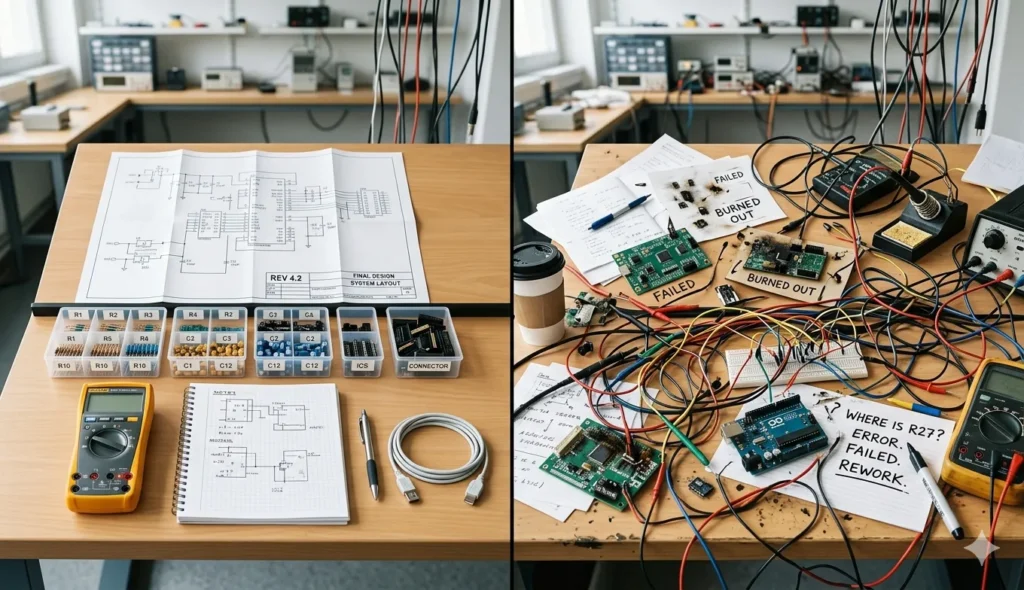
A well-planned PCB design process is structured, efficient, and predictable. It minimizes risks by addressing potential issues early and ensures that all design aspects are aligned. Engineers who follow a systematic approach can deliver high-quality products within budget and on schedule. Planning also improves communication between teams, leading to better collaboration and fewer misunderstandings during development.
In contrast, unplanned PCB design is chaotic and reactive. Issues are discovered late, leading to costly redesigns and delays. This approach often results in poor performance, unreliable products, and increased stress for engineering teams. Companies that rely on unplanned processes struggle to maintain consistency and competitiveness in the market.
Comparison Table
| Aspect | Planned Design | Unplanned Design |
|---|---|---|
| Development Time | Optimized and predictable | Delayed and inconsistent |
| Cost | Controlled and efficient | High and unpredictable |
| Product Quality | High reliability | Frequent issues |
| Team Collaboration | Strong and aligned | Miscommunication |
| Risk Level | Low | High |
Short Paragraph:
This comparison clearly shows that proper planning is not just beneficial—it is essential for achieving success in PCB design.
Building a Robust PCB Design Workflow
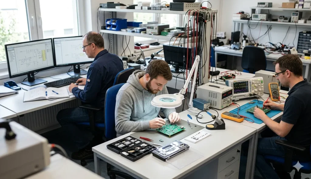
Creating a reliable PCB requires a structured workflow that integrates planning, design, testing, and validation. Each stage should be clearly defined, with specific goals and deliverables. This ensures that the design process is organized and efficient, reducing the likelihood of errors and rework. A well-defined workflow also helps teams stay aligned and focused on achieving project objectives.
Another important aspect of a robust workflow is continuous improvement. Engineers should analyze past projects to identify areas for improvement and implement best practices in future designs. This iterative approach enhances efficiency and ensures that designs become more reliable over time. By learning from previous experiences, teams can avoid repeating mistakes and achieve better results.
Automation tools and design software also play a crucial role in modern PCB development. They help streamline processes, improve accuracy, and reduce manual effort. Integrating these tools into the workflow enhances productivity and allows engineers to focus on innovation rather than repetitive tasks.
Hardware Development Process Matrix
A structured workflow ensures consistency and reduces the chances of errors during the design process.
Continuous improvement helps teams refine their approach and deliver better results over time
Using modern tools enhances efficiency and enables engineers to focus on innovation and quality.
Long-Term Benefits of Proper Planning

Proper PCB planning provides long-term benefits that extend beyond the initial design phase. It ensures product reliability, reduces maintenance costs, and improves customer satisfaction. Well-designed PCBs are easier to scale and adapt to future requirements, making them ideal for evolving technologies. Companies that invest in planning gain a competitive advantage by delivering high-quality products consistently.
In addition, proper planning supports regulatory compliance and certification processes. Meeting industry standards is essential for entering global markets and avoiding legal issues. A well-planned design simplifies compliance testing and reduces the risk of failure. This not only saves time but also enhances the credibility of the product in the market.
Reliable designs lead to better customer experiences and stronger brand reputation.
Scalable solutions allow businesses to adapt to changing market demands
Compliance readiness ensures smooth entry into international markets.
Final Thoughts
Avoiding costly mistakes in PCB design starts with proper planning and a structured approach. Engineers must prioritize system-level thinking before moving into design.
Investing time in planning reduces risks, saves costs, and improves product quality. It ensures that designs are reliable and ready for real-world applications.
By following best practices and focusing on early validation, teams can achieve successful PCB designs and long-term business growth.