












Introduction
A small black chip with eight pins can control an LED flasher, generate a clock signal or switch a circuit after a fixed delay. That is what makes the 555 Timer IC so useful. It provides a simple way to build timing and pulse-generation circuits without programming a microcontroller.
The timing comes from an external resistor-capacitor network. Inside the chip, comparators monitor voltage levels and an internal flip-flop controls the output. Change the resistor or capacitor values and the circuit behaves differently.
You will usually encounter the 555 in astable and monostable circuits. It also works as a bistable latch, PWM generator and Schmitt trigger. Those configurations make it useful for far more than a basic blinking LED.
This article starts with the pin configuration and internal working, then moves through the three common operating modes. You will also build a practical LED flasher, see its timing calculated and learn about additional applications and common faults.
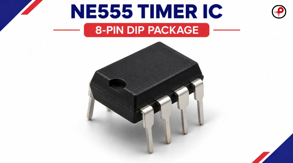
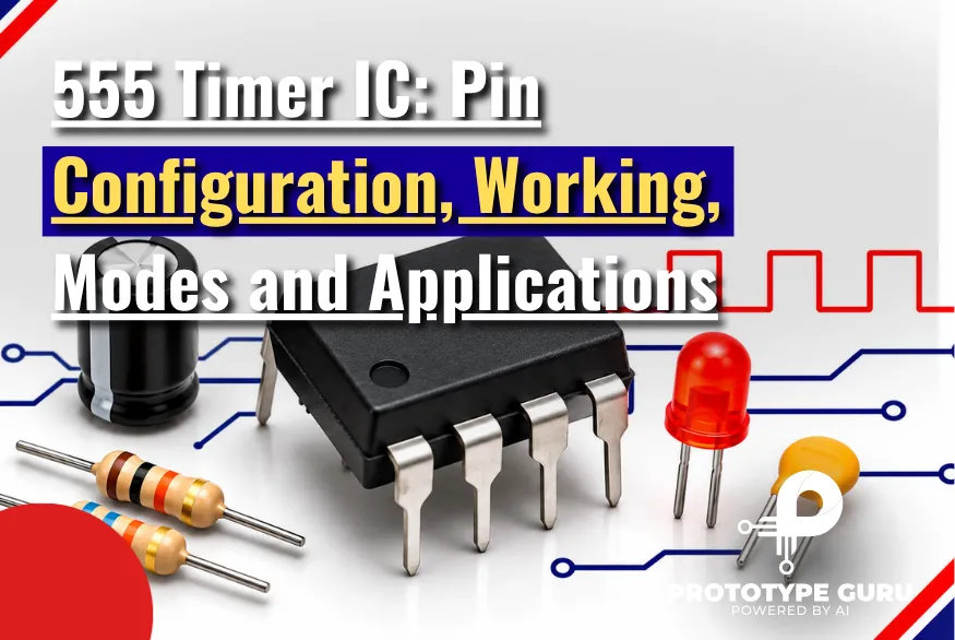
Image placement: Add a clean product-style image of an NE555 Timer IC in an 8-pin DIP package. Make the chip marking and all eight metal pins visible. Use a simple background without extra labels or decorative elements.
1. What Is a 555 Timer IC?
The 555 Timer IC is an integrated circuit used to generate time delays, pulses and oscillating signals. It monitors voltage at its input pins and changes the output when those voltages cross specified levels. External resistors and capacitors determine the timing.
The device became popular because a basic circuit needs very few components. Connect a resistor and capacitor in the correct arrangement and the same IC can produce a timed output or a repeating waveform.
A standard bipolar NE555 contains eight pins. Its internal circuit includes a voltage divider, two comparators, an SR flip-flop, a discharge transistor and an output stage. Each part has a specific job in controlling the timer.
The external capacitor stores and releases charge through the resistor network. That changing voltage is what makes the timer switch. Increasing the capacitance generally lengthens the timing interval, while changing resistance alters the charging and discharging periods.
Main Features of the 555 Timer IC
The NE555 offers several useful features:
- Eight-pin integrated circuit.
- Astable and monostable timing operation.
- Can be connected as a bistable latch.
- External resistor-capacitor timing control.
- Dedicated trigger, threshold and reset inputs.
- Control-voltage input for adjusting reference levels.
- Output stage capable of sourcing or sinking current within its ratings.
The NE555 uses bipolar technology. CMOS alternatives include the TLC555 and ICM7555. They share the same basic timing principle, but their supply voltage, current consumption and output-drive characteristics are different. Check the exact part number before replacing one with another.
2. 555 Timer IC Pin Configuration
The standard 555 Timer IC has eight pins. They handle the power supply, trigger signal, threshold detection, reset control, discharge path and output.
For the common 8-pin DIP package, hold the chip with its semicircular notch facing upward. Pin 1 sits at the upper-left corner. Count counterclockwise around the package to identify the remaining pins.
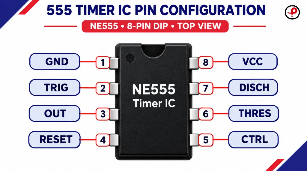
Image placement: Add a verified top-view pinout diagram of the 8-pin NE555 package. Show the notch, pin numbers 1 through 8 and their names. Check the orientation carefully before adding the image to the article.
Functions of the 555 Timer IC Pins
| Pin | Name | Function |
|---|---|---|
| 1 | GND | Ground connection for the power supply. |
| 2 | TRIG | Trigger input. A voltage below approximately one-third of VCC sets the internal flip-flop. |
| 3 | OUT | Provides the timer’s output signal. |
| 4 | RESET | Active-low reset input. Pulling it LOW forces the output LOW. |
| 5 | CTRL | Control-voltage input. It adjusts the internal reference levels. |
| 6 | THRES | Threshold input. It monitors the timing voltage and resets the flip-flop when the upper threshold is crossed. |
| 7 | DISCH | Discharge connection for the external timing capacitor. |
| 8 | VCC | Positive power supply connection. |
Important Pin Connections
Connect pin 1 to ground and pin 8 to the positive supply. When you do not need an external reset signal, connect pin 4 to VCC. Leaving RESET LOW would keep the output in its reset state.
Pin 5 controls the internal reference voltages. In an ordinary timing circuit, a 10 nF capacitor from this pin to ground helps filter unwanted noise. If you intend to use voltage control or PWM, follow the relevant circuit instead of treating pin 5 as an unused connection.
Pins 2 and 6 are joined in the standard astable circuit. They monitor the same timing capacitor, allowing the timer to switch as the capacitor charges and discharges.
Pin 7 connects to the timing resistor network. Its internal discharge transistor provides a path to ground when the timer output is LOW.
The exact wiring changes with the operating mode. Use the circuit diagram for your chosen configuration rather than assuming every pin has the same external connection in every project.
3. How Does a 555 Timer IC Work?
Inside a standard 555 timer, a voltage divider establishes two reference levels. The lower reference is approximately one-third of VCC, and the upper reference is approximately two-thirds of VCC.
The trigger comparator monitors pin 2. When its voltage falls below the lower reference, it sets the internal flip-flop and the output goes HIGH. The threshold comparator monitors pin 6. When that voltage rises above the upper reference, it resets the flip-flop and the output goes LOW.
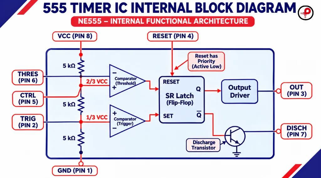
Image placement: Add an original technical block diagram showing the three equal divider resistors, two comparators, SR flip-flop, discharge transistor and output stage. Label the one-third VCC and two-thirds VCC reference levels. Verify every signal path against the NE555 datasheet.
Main Internal Components
Voltage divider
Three equal resistors are connected internally between VCC and ground. They create the one-third and two-thirds supply-voltage reference levels used by the comparators.
Comparators
The two comparators check the trigger and threshold inputs against their reference levels. Their outputs determine whether the flip-flop should be set or reset.
SR flip-flop
The flip-flop remembers the timer’s current state. A valid trigger sets it, while the threshold comparator or active-low RESET input can reset it. Its state controls the output stage and discharge transistor.
This arrangement is a useful example of analog voltage levels controlling a digital-style output, a concept also explored in analog and digital circuit design.
Discharge transistor
The discharge transistor connects internally to pin 7. When it turns ON, the timing capacitor gets a path to ground. When it turns OFF, the external resistor network can charge the capacitor.
Output stage
Pin 3 is driven by the output stage. It can source or sink current within the device’s electrical limits. A motor or another high-current load should use an appropriate transistor, MOSFET or driver rather than relying directly on the timer output.
Following One Timing Cycle
Imagine a capacitor connected to the trigger and threshold inputs. At the start of an astable cycle, the capacitor voltage is low. Once it is below one-third of VCC, the trigger comparator sets the flip-flop.
The output goes HIGH. The discharge transistor switches OFF, so current can flow through the external resistor network and charge the capacitor.
As the capacitor voltage rises past two-thirds of VCC, the threshold comparator resets the flip-flop. Pin 3 goes LOW and the discharge transistor turns ON. The capacitor then discharges through the timing resistor.
Once its voltage drops below the lower reference, the trigger comparator sets the flip-flop again. The cycle starts over. A monostable circuit uses the same internal action but stops after its timed pulse instead of repeating continuously.
4. Operating Modes of the 555 Timer IC
The three basic configurations are astable, monostable and bistable. Each uses the internal flip-flop differently. The external resistor, capacitor and input connections determine whether the output repeats, produces one pulse or holds its last state.
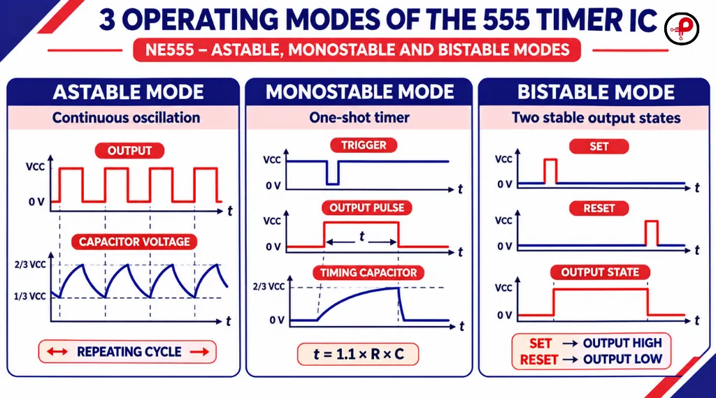
Image placement: Add a three-panel comparison graphic. Show a continuous square wave for astable mode, one triggered pulse for monostable mode, and two stable output states for bistable mode. Keep this as an overview; detailed circuit diagrams will follow.
4.1 Astable Mode
An astable circuit has no stable output state. The 555 keeps switching between HIGH and LOW while power is applied, producing a continuous square wave. This is why the configuration is also called an astable multivibrator.
The standard circuit uses two resistors, RA and RB, with one timing capacitor. The capacitor charges through both resistors and discharges through RB. Changing their values changes the frequency and the time spent in each output state.
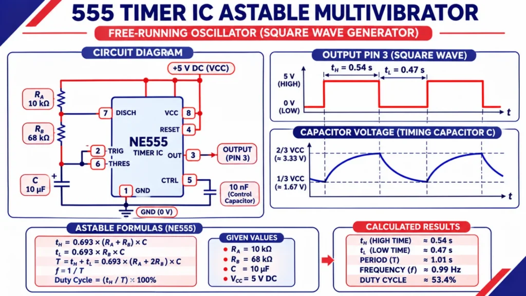
Image placement: Add a verified astable circuit schematic with RA, RB and the timing capacitor. Show pins 2 and 6 joined, the correct pin 7 resistor path, the output square wave and the capacitor voltage waveform.
How Astable Mode Works
When the supply is connected, the capacitor starts charging through RA and RB. Its voltage rises towards the upper reference level, approximately two-thirds of VCC.
At that point the threshold comparator resets the flip-flop, making the output LOW. The discharge transistor turns ON and the capacitor releases its charge through RB.
The voltage eventually falls below one-third of VCC. The trigger comparator sets the flip-flop, the output becomes HIGH and the discharge transistor turns OFF. Charging starts again.
This process continues until the circuit is switched off or reset.
Astable Mode Timing Formulas
The standard two-resistor circuit uses the following approximate equations.
Output HIGH time:
[
t_H = 0.693(R_A+R_B)C
]
Output LOW time:
[
t_L = 0.693R_BC
]
Total time period:
[
T = t_H+t_L
]
Output frequency:
[
f \approx \frac{1.44}{(R_A+2R_B)C}
]
Duty cycle:
[
D = \frac{R_A+R_B}{R_A+2R_B}\times100%
]
Where:
- (R_A) and (R_B) are timing resistors in ohms.
- (C) is the timing capacitor in farads.
- (t_H) is the output HIGH duration.
- (t_L) is the output LOW duration.
- (T) is the complete cycle time.
- (f) is the output frequency.
- (D) is the percentage of the cycle spent HIGH.
In this standard arrangement, the duty cycle is above 50% because charging takes place through both resistors, while discharging uses RB alone. A diode modification can create separate charging and discharging paths and allow a different duty-cycle range. Use equations for that modified circuit rather than applying the standard ones unchanged.
Where Astable Mode Is Used
You can use an astable 555 for a blinking indicator, a basic clock signal, a tone generator or a repeating alarm. It also makes a useful demonstration circuit because the effect of changing RA, RB or C is easy to observe.
4.2 Monostable Mode
A monostable circuit has one stable state. A trigger temporarily changes the output to HIGH, and the timer returns it to LOW when the timing interval ends.
This is also known as a one-shot circuit. It is useful when a button press, sensor event or another input needs to produce an output pulse of a known duration.
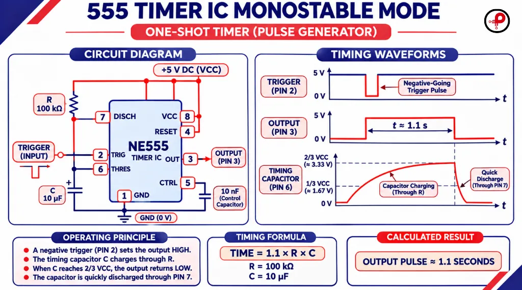
Image placement: Add a verified monostable schematic showing the trigger input, timing resistor, timing capacitor and output. Include the capacitor charging waveform and the single output pulse. Show the suitable negative-going trigger pulse.
How Monostable Mode Works
Before triggering, the output is LOW and the discharge transistor keeps the timing capacitor discharged. A negative-going pulse at pin 2 takes the trigger voltage below one-third of VCC. The flip-flop is set and the output goes HIGH.
The discharge transistor turns OFF. The capacitor can now charge through the timing resistor. When its voltage reaches approximately two-thirds of VCC, the threshold comparator resets the flip-flop. The output returns LOW and the capacitor discharges.
The circuit is then ready for another trigger. For the normal timing cycle, the trigger input must return HIGH before the timing interval ends. Holding it LOW can prevent the output from returning LOW as expected.
Monostable Timing Formula
The pulse duration can be estimated using:
[
T = 1.1RC
]
Here, (R) is the timing resistance in ohms and (C) is the capacitance in farads. The result is in seconds.
For example, use a 100 kΩ resistor with a 10 µF capacitor:
[
T = 1.1 \times 100000 \times 0.00001
]
[
T \approx 1.1\text{ seconds}
]
The output should remain HIGH for about 1.1 seconds after a valid trigger. Real measurements can differ slightly because resistors and capacitors have tolerances. Electrolytic capacitor leakage can also affect longer intervals.
Where Monostable Mode Is Used
Monostable circuits are used for push-button delays, switch debouncing, short control pulses and sensor-triggered indicators. They are also useful when a circuit needs a fixed activation period after an input event.
4.3 Bistable Mode
In bistable mode, the 555 timer acts as a set-reset latch. It has two stable output states, HIGH and LOW, and stays in the selected state until another input changes it.
There is no timing capacitor setting a fixed pulse duration. Two external controls determine the state: the trigger input sets the output, and the RESET input clears it.
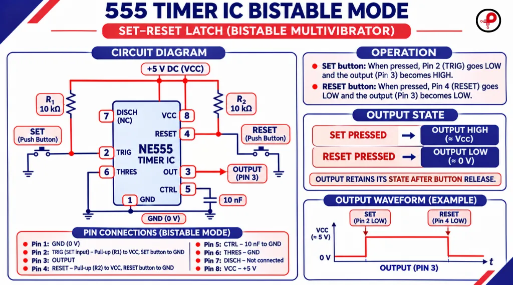
Image placement: Add a verified bistable/latch schematic. Show separate SET and RESET push buttons, pull-up resistors on pins 2 and 4, pin 6 tied to ground, pin 7 unused, pin 5 bypassed with a small capacitor, and the output at pin 3.
How Bistable Mode Works
In a common latch circuit, pull-up resistors keep pins 2 and 4 HIGH. Pressing the SET button briefly connects pin 2 to ground. The trigger comparator sets the flip-flop and pin 3 goes HIGH.
Pressing the RESET button pulls pin 4 LOW. The reset input overrides the normal trigger and threshold operation, clearing the flip-flop and taking the output LOW.
For this arrangement, pin 6 is connected to ground so the threshold comparator does not end the HIGH state. Pin 7 is not used as a timing discharge connection. A small capacitor from pin 5 to ground helps keep the control input quiet.
The output remains in its selected state after the button is released. The circuit therefore works as a simple electronic ON/OFF latch. Add a defined power-up reset if the output must always start in a known state.
5. 555 Timer IC Circuit Diagram: LED Flasher Project
An LED flasher is a good first project because the output is visible and the timing can be checked with simple tools. This example uses the NE555 in astable mode. The two resistors and capacitor set the flash rate.
Use a regulated 5V supply for the circuit. A stable supply helps prevent unwanted changes in timing and false triggering. Choosing a suitable power supply for embedded systems is part of getting a reliable circuit.
Components Required
| Component | Quantity | Example value |
|---|---|---|
| NE555 Timer IC | 1 | NE555 |
| Timing resistor RA | 1 | 10 kΩ |
| Timing resistor RB | 1 | 68 kΩ |
| Timing capacitor | 1 | 10 µF |
| LED current-limiting resistor | 1 | 1 kΩ |
| LED | 1 | Standard LED |
| DC power supply | 1 | Regulated 5V |
| Supply bypass capacitor | 1 | 100 nF |
| Control-pin capacitor | 1 | 10 nF |
| Breadboard and jumper wires | As required | — |
Circuit Connections
Start by connecting pin 1 to ground and pin 8 to the positive 5V supply. Pin 4 also connects to 5V so the timer remains out of reset during normal operation.
Join pins 2 and 6. Connect RA between the positive supply and pin 7. RB goes between pin 7 and the joined pins 2 and 6. This creates the charging and discharging path used in astable operation.
Connect the 10 µF capacitor between the joined timing node and ground. For an electrolytic capacitor, its positive terminal goes to the timing node and its negative terminal goes to ground.
Connect pin 3 to the LED through the 1 kΩ resistor. Place the LED in the correct polarity, with its cathode towards ground. Add a 10 nF capacitor from pin 5 to ground. Place the 100 nF bypass capacitor close to the IC, directly between pins 8 and 1. Short supply connections and suitable bypassing help reduce noise; see our guide to power supply filtering.
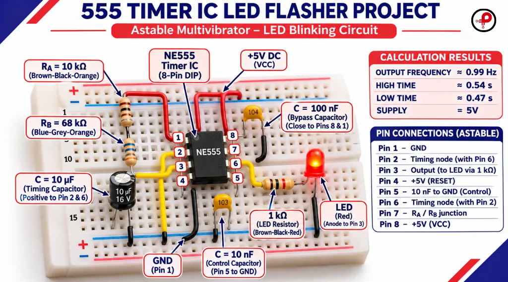
Image placement: Add a realistic breadboard illustration showing the NE555, 10 kΩ and 68 kΩ timing resistors, 10 µF capacitor, LED, 1 kΩ resistor, 10 nF control capacitor, 100 nF bypass capacitor and 5V supply. The physical layout must match the verified schematic and connections above.
How the LED Flasher Works
After power is applied, the timing capacitor charges through RA and RB. When it reaches the upper reference level, the output changes state and the discharge transistor turns ON. The capacitor then discharges through RB.
Once the voltage falls below the lower reference, the output goes HIGH again. The LED follows the output signal and flashes repeatedly while the circuit remains powered.
Calculating the Flashing Frequency
For this example:
- (R_A = 10,k\Omega)
- (R_B = 68,k\Omega)
- (C = 10,\mu F)
The HIGH time is:
[
t_H = 0.693(10000+68000)(0.00001)
]
[
t_H \approx 0.54\text{ seconds}
]
The LOW time is:
[
t_L = 0.693(68000)(0.00001)
]
[
t_L \approx 0.47\text{ seconds}
]
The complete period is approximately 1.01 seconds, giving a frequency close to 0.99 Hz. The LED therefore completes roughly one flash cycle each second.
These are calculated estimates, not guaranteed measured values. Component tolerance and capacitor leakage affect the actual timing. An oscilloscope connected to pin 3 will show the output waveform and allow you to measure the real frequency.
Before switching on: Check the supply polarity, LED direction, capacitor orientation and all eight IC pin connections. Keep the LED’s current-limiting resistor in place. For motors or other high-current loads, use a suitable driver stage.
6. Other Useful 555 Timer IC Applications
The three basic modes are only part of what the 555 can do. The control-voltage pin and the two comparator thresholds allow other useful circuit arrangements.
Pulse-Width Modulation (PWM)
PWM controls the fraction of each cycle that an output remains HIGH. That fraction is called the duty cycle. Changing it changes the average voltage delivered by a switching circuit.
A 555 timer can generate PWM by using a continuous pulse train to trigger a monostable circuit. An external control signal applied to pin 5 changes the internal threshold voltage, which changes the width of the output pulses.
This arrangement needs a suitable input pulse train and timing network. The relationship between the control voltage and pulse width is not linear because the timing capacitor charges through an RC network. Do not assume that a 50% change in control voltage produces a 50% change in pulse width.
Schmitt Trigger
A 555 timer can work as a Schmitt trigger by connecting pins 2 and 6 together and applying the input signal to their common connection. The output switches LOW when the input rises above approximately two-thirds of VCC. It switches HIGH again after the input falls below approximately one-third of VCC.
The gap between those switching levels is called hysteresis. It prevents the output from changing repeatedly when a noisy or slowly changing signal sits near a single threshold.
This circuit can be used to clean up a slow signal from a sensor or convert a changing voltage into a more definite HIGH or LOW output. The input and output waveforms are worth showing in a separate experiment. A worked example is available in this 555 timer Schmitt trigger circuit reference.
Missing-Pulse Detector
A missing-pulse detector checks whether a repeating input signal continues to arrive within a set time. The 555 is arranged as a retriggered monostable circuit. Each incoming pulse restarts the timing interval.
As long as the pulses arrive within that interval, the timer keeps resetting its timing cycle. When a pulse is missing, or the gap becomes too long, the timing period finishes and the output produces a fault indication.
There is an important limitation in TI’s example circuit: the missing-pulse fault must be represented by a HIGH input. A signal stuck LOW is not detected by that particular arrangement because the timing capacitor remains discharged. Check the input polarity and circuit design before using it as a protection function.
Sequential Timers and Pulse Generators
A 555 can produce a timed output that triggers a second timer stage. Connecting stages in sequence creates a simple delay pattern, such as switching one output after another. The timing of each stage is set by its own resistor-capacitor network.
The IC is also used in pulse-shaping circuits, frequency dividers and pulse-position modulation. These applications need circuit arrangements designed for the particular input and timing requirements. They are not all achieved by simply changing the two resistors in a standard LED flasher.
7. 555 Timer IC Specifications and Characteristics
Specifications depend on the exact manufacturer and part number. The following values refer to the Texas Instruments NE555, not every device sold under the general 555 timer name.
NE555 Key Specifications
| Parameter | Texas Instruments NE555 |
|---|---|
| Number of pins | 8 |
| Recommended supply voltage | 4.5V to 16V |
| Supply range used for specified electrical characteristics | 5V to 15V |
| Typical supply current | Approximately 2 mA |
| Output current | Up to ±200 mA under specified conditions |
| Operating temperature | 0°C to 70°C |
| Timing operation | Astable and monostable |
The supply ranges in the table describe different things. TI lists 4.5V to 16V as the recommended operating range for the NE555. Its product documentation also states that operation is specified for supplies from 5V to 15V. Use the datasheet conditions when checking the limits of a particular design.
The output stage can source or sink up to 200 mA under specified conditions. This is a device capability, not a target current for every circuit. Output voltage drop, package heating and the connected load all matter. Follow the electronic component derating guidelines when selecting operating conditions.
The NE555 listed by TI has an operating temperature range of 0°C to 70°C. Other members of the xx555 family have different temperature ratings, so do not transfer a rating from the SE555 or SA555 to the NE555.
Power dissipation depends on the package and operating conditions. Check the manufacturer’s thermal data when the output is heavily loaded or the ambient temperature is high.
Bipolar NE555 vs CMOS TLC555
The traditional NE555 is a bipolar timer. The TLC555 is a CMOS alternative from Texas Instruments. Both use the same basic timing principle and have compatible pin functions, but their electrical characteristics differ.
| Parameter | TI NE555 | TI TLC555 |
|---|---|---|
| Technology | Bipolar | CMOS |
| Recommended supply voltage | 4.5V–16V | 2V–15V |
| Typical supply current | About 2 mA | About 0.18 mA |
| Operating temperature | 0°C–70°C | -40°C–125°C |
The TLC555 draws much less supply current, making it worth considering for battery-powered equipment. Its output-drive characteristics are also different. TI lists typical sink current of 100 mA and typical source current of 10 mA for the TLC555, rather than the NE555’s stated output capability.
When choosing between bipolar and CMOS versions, compare the supply, current, temperature and output requirements. Good electronic component selection prevents an apparently interchangeable replacement from causing problems in the finished circuit. For battery-powered equipment, the principles in our low-power circuit design guide are also relevant.
8. Common 555 Timer IC Problems and Troubleshooting
A timer circuit that does not work usually has a wiring issue, an incorrect component value or an input signal that is not reaching the required voltage. Check the circuit in a logical order before replacing the IC.
The Output Does Not Change
Measure the supply voltage between pins 8 and 1. Check that pin 4 is HIGH when reset is not being used. Then inspect pin 2 and pin 6. In astable operation, both should connect to the timing node.
The LED Stays On or Off
Check the LED polarity and the resistor in series with it. Measure pin 3 to see whether the output is switching. If it stays in one state, check the timing capacitor voltage and the connections around pins 2, 6 and 7.
The Flashing Rate Is Incorrect
Read the resistor and capacitor markings again. A 10 µF capacitor with a broad tolerance can produce a noticeable timing difference. Also check for leakage, poor breadboard contacts and incorrect wiring around pin 7.
The Circuit Triggers Unexpectedly
Noise can enter through long wires, a poor ground connection or the control-voltage pin. Fit the 100 nF supply bypass capacitor close to pins 8 and 1. A 10 nF capacitor from pin 5 to ground is commonly used when external control voltage is not required.
The IC Becomes Hot
Switch off the supply and inspect the load connected to pin 3. Motors, relays and other demanding loads should use a suitable driver. Check the current drawn from the output and make sure the IC is being operated within its specified limits.
Frequently Asked Questions
What does a 555 Timer IC do?
A 555 Timer IC generates time delays, pulses and repeating signals. External resistors and capacitors set its timing, while internal comparators and a flip-flop control the output.
What are the three common modes of a 555 timer?
They are astable, monostable and bistable. Astable mode produces a repeating waveform, monostable mode generates one timed pulse after a trigger, and bistable mode holds its last selected output state.
What is the supply voltage of an NE555?
For the Texas Instruments NE555, the recommended supply range is 4.5V to 16V. Its electrical characteristics are specified over stated test conditions, including 5V to 15V. Always check the datasheet for your exact part.
Can a 555 timer generate PWM?
Yes. An external pulse train can trigger a monostable timer while a control signal at pin 5 changes the threshold voltage and pulse width. The circuit needs to be designed for the required frequency and duty-cycle range.
Can I connect a motor directly to a 555 timer?
A motor should normally be controlled through a transistor, MOSFET or motor-driver circuit. Check the motor’s starting current and the driver’s rating before connecting it to the timer output.
Conclusion
The 555 Timer IC can handle a surprising range of timing and switching jobs with a small external circuit. Its comparators and flip-flop provide the switching action, while resistors and capacitors determine the timing.
The astable, monostable and bistable arrangements cover the usual starting points. With suitable external connections, the same device can also generate PWM, clean up slow signals with Schmitt-trigger action or detect a missing pulse.
For a dependable build, follow the pin connections, calculate the timing components and check the datasheet for the exact device. A bipolar NE555 and a CMOS TLC555 may look interchangeable, but their current and operating limits are not the same.
References
- Texas Instruments: NE555 product page and technical documentation
- Texas Instruments: xx555 Precision Timers datasheet, Revision K
- Texas Instruments: TLC555 CMOS Timer product page and datasheet
- Ray Marston, Nuts & Volts: Using the 555 Timer IC in Special or Unusual Circuits