







I have spent more than eight years working across analog front ends, digital logic boards, and the messy middle ground where the two meet. If there is one thing I have learned, it is that analog and digital circuit design is not really two separate skills. It is one continuous spectrum, and almost every product I have shipped needed both.
A pressure sensor produces a tiny analog voltage. Somewhere downstream, a microcontroller needs that value as a clean digital number so firmware can act on it. A digital audio file needs to become a smooth analog waveform before it reaches a speaker. That translation, back and forth between continuous and discrete worlds, is the daily work of hardware engineering.
This guide walks through analog circuit design, digital circuit design, CMOS technology, mixed signal circuit design, VLSI design, and how all of it comes together on a printed circuit board. I have tried to write it the way I would explain it to a junior engineer on my team, with enough depth that a working professional still gets value out of it.
By the end, you will understand how analog and digital circuits differ, when to choose one approach over the other, how to avoid the mistakes that trip up most beginners, and what a real design workflow looks like from schematic to finished board.
What Is Analog and Digital Circuit Design
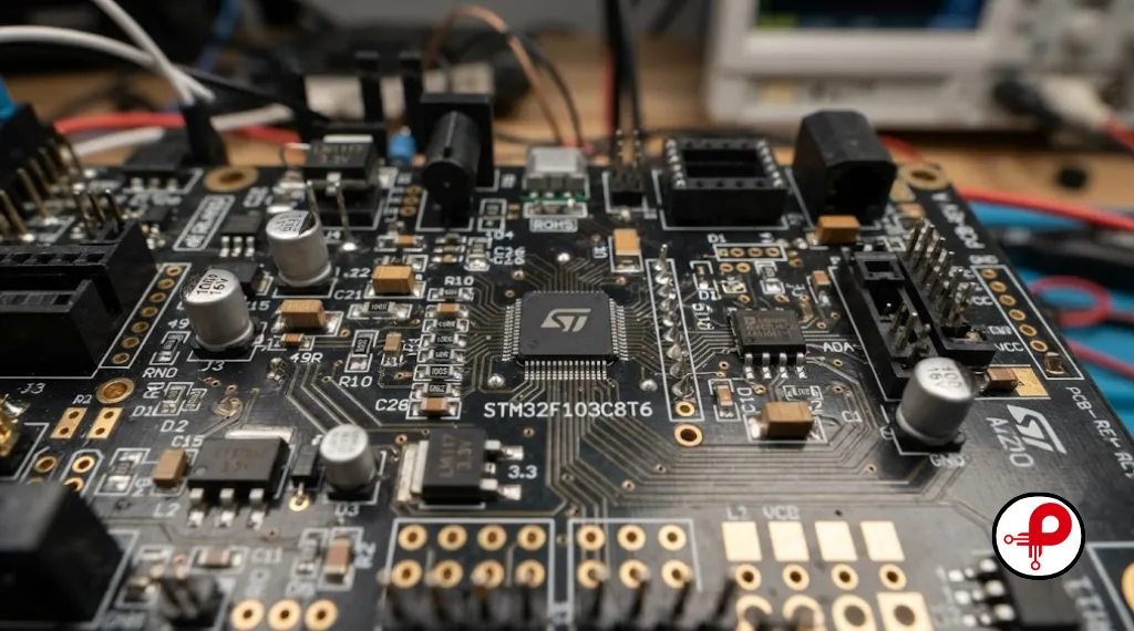
Analog and digital circuit design is the process of creating electronic circuits that manipulate electrical signals to perform a function, whether that is amplifying a sound wave, switching a motor, or running the logic inside a processor.
Analog circuit design deals with continuous signals, voltages and currents that can take any value within a range. Digital circuit design deals with discrete signals, values that only exist as one of two logic states, commonly represented as 0 and 1.
Both disciplines share the same underlying physics and many of the same components, but they demand different mindsets, different tools, and different layout rules once you move to a physical board. A design engineer who understands both is far more valuable than one who only knows a single side of the spectrum, because almost no modern product is purely one or the other.
Analog Circuit Design Explained
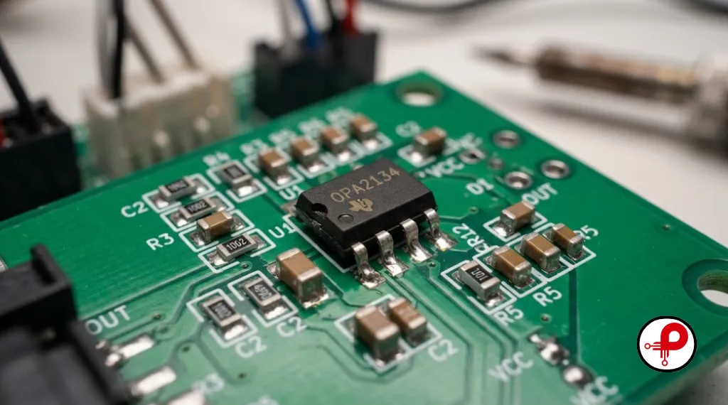
Analog circuit design is often described as more of a craft than a formula, and in my experience that description holds up. There is rarely a single correct answer to an analog problem. Ask five experienced analog engineers to design the same amplifier stage and you will likely get five different topologies, each with its own tradeoffs.
What Analog Circuits Do
Analog circuits process signals that vary smoothly over time, similar to a dimmer switch instead of an on off light switch. Common analog building blocks include:
Including the operational amplifier design used in nearly every analog front end.
Shape frequency content using resistors, capacitors, and inductors.
Generate periodic waveforms for timing or signal generation.
Voltage regulators and power management circuits.
Sensor interface circuits that condition weak, noisy signals from the physical world.
Why Analog Circuit Design Is Difficult
Analog circuit design basics start simple, Ohm’s law, voltage dividers, RC time constants, but the difficulty grows quickly once you factor in component tolerances, temperature drift, parasitic capacitance, and noise. A resistor on paper is a perfect resistor. A real resistor has tolerance, temperature coefficient, and parasitic inductance that only matters once you are chasing a noise floor at two in the morning before a deadline.
This is why analog circuit design typically takes longer per function than digital design, and why experienced analog engineers remain in high demand even as automated tools have improved. Custom IC design services and boutique analog design houses still rely heavily on engineers who have built intuition over years of hands on iteration.
Digital Circuit Design Explained
Digital circuit design works with binary logic, values that are either high or low, one or zero, true or false. This constraint sounds limiting, but it is exactly what makes digital circuits so much easier to scale, automate, and verify.
What Digital Circuits Do
Digital circuit design techniques rely on combinations of logic gates such as AND, OR, NOT, and XOR, built up into more complex structures like:
Flip-flops & Registers
Store single bits of data reliably across clock cycles.
Counters & State Machines
Sequence complex operations and transitions over time.
Microcontrollers & Microprocessors
Execute stored instructions for flexible computing control.
FPGA Circuit Development
Configure custom logic dynamically in reprogrammable hardware.
ASIC Design Flow
Custom-fabricate optimized logic for high-performance applications.
System Integration
Combine multiple digital and analog blocks into a unified operational system.
Why Digital Design Scales Better
Because digital signals only need to be recognized as high or low rather than measured with precision, digital circuits tolerate noise far better than analog circuits. A small voltage fluctuation on a digital line rarely changes whether it reads as a 1 or a 0. That noise margin is a big part of why digital electronics design has scaled from a handful of transistors to processors with tens of billions of transistors, something that would be essentially impossible with equivalent analog complexity.
Automated design tools, hardware description languages, and standardized cell libraries also mean digital circuits can be synthesized, simulated, and verified with a level of automation that analog design still cannot fully match. This is the main reason digital IC design techniques have advanced so much faster than analog techniques over the last three decades.
Analog vs Digital Circuit Design: Key Differences
Understanding analog vs digital circuit design comes down to a handful of core distinctions. Here is a side by side comparison I use when training new engineers.
| Factor | Analog Circuit Design | Digital Circuit Design |
|---|---|---|
| Signal type | Continuous, infinite values within a range | Discrete, two logic states (0 and 1) |
| Noise sensitivity | High, small voltage shifts change meaning | Low, wide noise margins between states |
| Design approach | Iterative, experience driven, less automated | Automated synthesis, simulation, and verification |
| Typical components | Op-amps, transistors, resistors, capacitors, inductors | Logic gates, flip-flops, microcontrollers, FPGAs, ASICs |
| Design time per function | Generally longer, requires careful tuning | Generally shorter, scales with EDA tooling |
| Precision | Directly represents real world values | Represents values in discrete steps, limited by resolution |
| Common failure mode | Drift, offset, noise coupling | Timing violations, metastability, signal integrity at high speed |
| Best suited for | Sensor interfaces, audio, RF, power supplies | Logic, memory, computation, communication protocols |
Neither approach is universally better. The right choice depends entirely on what the circuit needs to do. A temperature sensor front end almost always starts as analog, because temperature itself is a continuous physical quantity. The moment that measurement needs to be logged, transmitted, or compared against a threshold in software, it typically gets converted to digital.
Core Components Used in Both Design Disciplines
Regardless of whether you are working on analog or digital electronics design, every project relies on the same core building blocks. Components such as resistors, capacitors, inductors, transistors, diodes, integrated circuits, and power supplies form the foundation of reliable circuit design. A solid understanding of how these components interact allows engineers to create efficient, stable, and high performance electronic systems for applications ranging from consumer devices to industrial and embedded products.
1. Resistors
Limit current and set voltage division ratios, essential in both bias networks and pull up or pull down configurations on digital lines.
2. Capacitors
Store energy, filter noise, and set timing constants, used everywhere from power supply decoupling to analog filters.
3. Inductors
Store energy in a magnetic field, common in power converters and RF matching networks.
4. Diodes
Allow current flow in one direction, used for rectification, protection, and voltage referencing.
5. Bipolar Junction Transistors (BJT) and MOSFETs
Act as switches or amplifiers, forming the backbone of nearly every analog and digital circuit ever built.
6. Operational amplifiers
The workhorse of analog signal conditioning, used for gain, filtering, and signal buffering.
7. Logic gates and flip-flops
The fundamental digital building blocks that combine into everything from a simple counter to a full microcontroller core.
A solid grasp of these components, and how their non-ideal, real world behavior differs from the textbook model, is what separates a design that works on the bench from one that survives temperature extremes, manufacturing tolerance, and years of field use.
CMOS Technology in Modern Circuit Design
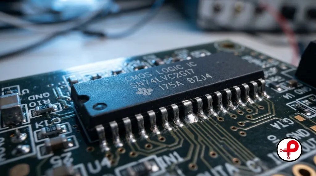
CMOS circuit design, short for complementary metal oxide semiconductor, is the dominant technology behind almost every digital chip made today, and it plays a major role in analog and mixed signal design as well.
CMOS technology pairs NMOS and PMOS transistors so that, in a steady logic state, almost no current flows through the gate. That property gives CMOS its defining advantage: extremely low static power consumption compared to older technologies like bipolar logic. This is a big reason battery powered devices, from wearables to smartphones, are built almost entirely on CMOS processes.
CMOS analog circuit design brings its own challenges. MOSFETs used in analog applications behave differently than the same devices used purely as digital switches, and analog CMOS design requires careful attention to threshold voltage variation, flicker noise, and matching between transistor pairs. Engineers working in CMOS analog circuit design often spend significant time on layout techniques like common centroid placement just to get two transistors to behave close enough to identically for a differential amplifier to work correctly.
As process nodes shrink, CMOS scaling has delivered smaller, faster, lower power digital logic generation after generation, but it has made analog CMOS design harder in some respects, since lower supply voltages leave less headroom for signal swing and noise margin.
Mixed Signal Circuit Design
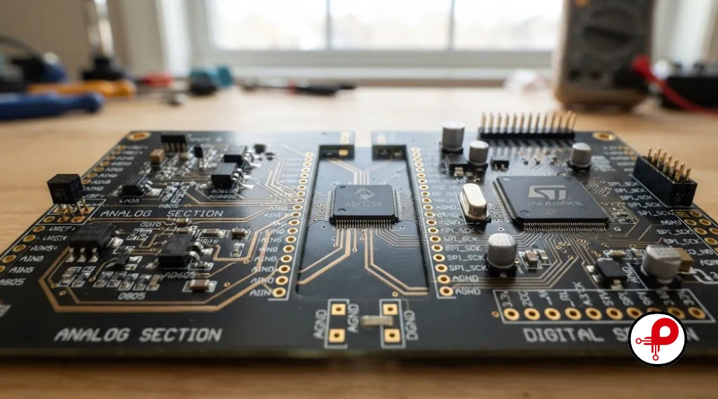
Mixed signal circuit design combines analog and digital circuits on the same PCB or integrated circuit, allowing them to work together as one system. Most modern electronic devices, including smartphones, medical equipment, automotive electronics, and IoT products, rely on mixed signal technology. In these systems, analog circuits capture and condition real world signals, while digital circuits process the information quickly and accurately. This combination delivers high performance, efficiency, and advanced functionality in compact electronic products.
A typical mixed signal system includes several essential building blocks. An analog front end receives signals from sensors, microphones, or antennas and prepares them for processing. An Analog to Digital Converter (ADC) transforms these analog signals into digital data that a microcontroller, FPGA, or processor can analyze. If an analog output is required, a Digital to Analog Converter (DAC) converts the processed data back into an analog signal. Stable and low noise power management circuits are also critical because they supply clean power to sensitive analog components while supporting high speed digital operations.
One of the biggest challenges in mixed signal circuit design is minimizing electrical noise between analog and digital sections. Fast digital switching can introduce interference that reduces analog signal accuracy if the PCB layout is not carefully planned. Successful designs use separate analog and digital power or ground areas, place ADCs and DACs near the boundary between both sections, and protect sensitive traces with proper shielding and grounding techniques. Following PCB layout recommendations from component manufacturers and using low noise voltage regulators helps engineers achieve reliable performance and accurate signal processing in mixed signal systems.
VLSI Circuit Design
VLSI design, or very large scale integration, refers to the process of creating integrated circuits containing hundreds of thousands to billions of transistors on a single chip. VLSI circuit design combines analog, digital, and mixed signal techniques at massive scale.
The VLSI design flow generally follows these stages:
Specification & Requirements
Define the high-level system requirements, performance targets (such as operating frequency and throughput), power consumption budgets, area constraints, and target application environment to establish clear engineering objectives.
Architecture Design
Partition the overall system into logical functional blocks, define internal bus protocols, memory hierarchies, data flow pipelines, and clock domains to optimize the chip for performance, power, and area (PPA).
RTL Design & Modeling
Describe the digital logic behavior and data transformations using Hardware Description Languages (HDLs) such as SystemVerilog, Verilog, or VHDL, ensuring the code is synthesizable and structurally clean.
Functional Verification
Simulate the RTL design extensively using testbenches, assertions, and UVM (Universal Verification Methodology) environments to verify protocol compliance, achieve high code coverage, and catch functional bugs early.
Logic Synthesis
Translate the Register-Transfer Level (RTL) code into an optimized gate-level netlist using EDA tools mapped against standard cell libraries from the chosen semiconductor foundry process node.
Physical Design & Layout
Execute floorplanning, power grid distribution, cell placement, clock tree synthesis (CTS), and global/detailed routing to map the logical netlist into physical transistor structures on the silicon die.
Sign-off & DRC/LVS Verification
Perform exhaustive static timing analysis (STA), power analysis, and physical verification checks including Design Rule Checking (DRC) and Layout Versus Schematic (LVS) to guarantee absolute reliability before tape-out.
Fabrication & Packaging
Generate final GDSII/OASIS mask data files, send them to a semiconductor foundry for wafer production, followed by silicon packaging, pin bonding, and rigorous post-silicon validation testing.
VLSI design underpins the ASIC design flow used to create custom chips for high volume products, as well as the FPGA circuit development flow used when engineers need reprogrammable digital hardware for prototyping or lower volume applications. Understanding VLSI design principles is genuinely useful even for engineers who mostly work at the board level, since it explains why certain chips behave, and cost, the way they do.
PCB Integration for Analog and Digital Circuits
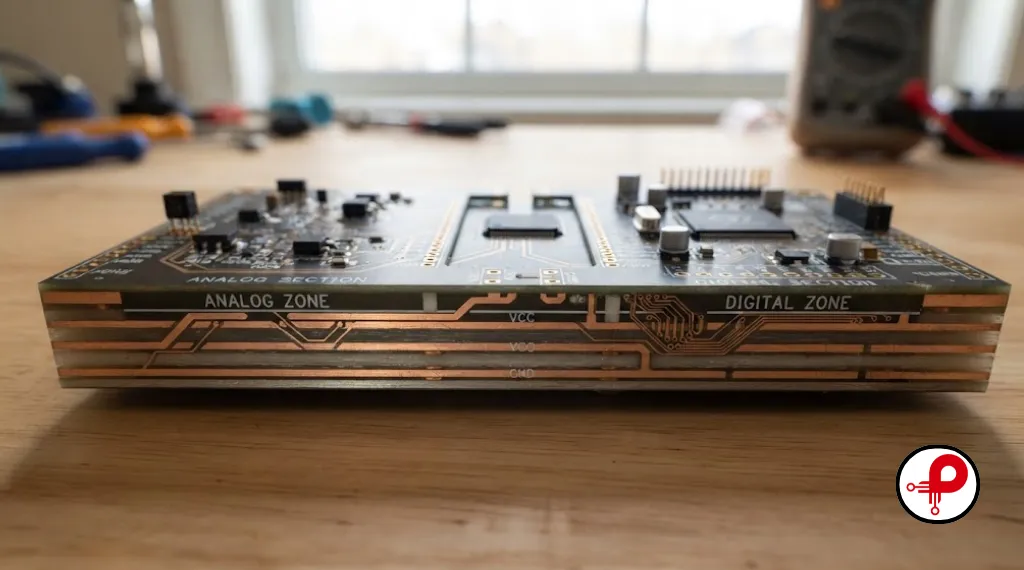
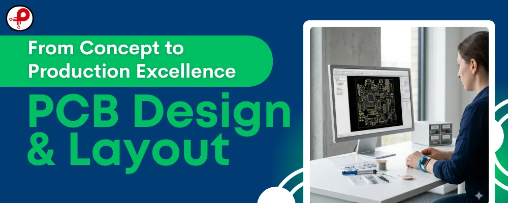
Getting analog and digital IC design right on paper is only half the job. PCB analog and digital design is where theory meets the physical world, and it is often where projects succeed or fail. A well planned PCB layout improves signal integrity, reduces electromagnetic interference, and ensures reliable communication between analog and digital sections. Understanding PCB design best practices early in the development process can prevent costly redesigns and improve overall product performance.
Key considerations for combining analog and digital circuits on one board include proper partitioning, grounding, signal routing, decoupling, thermal management, and EMI control. Engineers should physically separate analog and digital components, use an appropriate grounding strategy, and keep high speed digital traces away from sensitive analog signals. Following proven PCB design guidelines also helps achieve better performance, especially in high speed and mixed signal applications.
For projects that include wireless communication or high frequency electronics, additional design techniques become essential. Following best practices from our guides on 2.4 GHz PCB antenna design, thermal management in PCB design, PCB design vs PCB layout, and circuit board design rules can help improve signal quality, reduce noise, and increase long term reliability. These resources provide practical recommendations that complement analog and digital circuit design and help engineers build robust, production ready hardware.
The Circuit Design Process, Step by Step
Here is the workflow I follow on most projects, whether the end result is analog, digital, or mixed signal.
Define requirements
Nail down electrical specifications, environmental conditions, target cost, and regulatory requirements before touching a schematic tool.
Choose architecture
Decide how the system breaks into functional blocks and which parts will be analog, digital, or a converter boundary between them.
Select components
Pick specific parts based on performance, availability, and cost, an area where following solid guidelines prevents late-stage headaches.
Schematic capture
Draw the circuit in your chosen EDA tool, double checking pin assignments and power requirements against datasheets.
Simulation
Run SPICE simulations for analog sections and functional simulations for digital logic before committing to a layout.
PCB layout
Translate the schematic into a physical board, following partitioning and grounding practices covered earlier.
Design review
Have a second engineer review the schematic and layout, since a fresh set of eyes reliably catches mistakes.
Prototype and bring-up
Build a small batch, then power on and verify functionality methodically rather than testing everything at once.
Testing and validation
Confirm the board meets its original specifications across temperature, voltage, and load conditions.
DFM review
Check the design against your contract manufacturer’s capabilities before committing to production volume.
This overall flow mirrors what most experienced teams follow during an electronic product design workflow, regardless of whether the end product is a simple sensor board or a complex embedded system.
Applications of Analog and Digital Circuit Design
| Application Area | Primarily Analog | Primarily Digital | Typically Mixed Signal |
|---|---|---|---|
| Audio equipment | Amplification, filtering | Digital signal processing | Yes, ADC/DAC conversion |
| Medical devices | Sensor front ends | Data logging, display | Yes, especially wearable monitors |
| Industrial sensors | Signal conditioning | Communication protocols | Yes |
| Wearable technology | Battery management | Processing, wireless stack | Yes, heavily mixed signal |
| Automotive electronics | Power delivery, sensors | Control units, infotainment | Yes |
| Communication systems | RF front end | Baseband processing | Yes |
| Consumer electronics | Power supplies | Microcontrollers, memory | Yes |
| Test and measurement equipment | Precision analog inputs | Data processing and display | Yes |
Medical device development in particular tends to demand exceptionally careful mixed signal work, since patient safety depends on both accurate analog sensing and reliable digital processing working together without introducing noise or timing errors. The same is true for the growing development of wearable technology, where tiny form factors force analog and digital sections into extremely close physical proximity, making layout discipline even more critical.
Common Design Mistakes
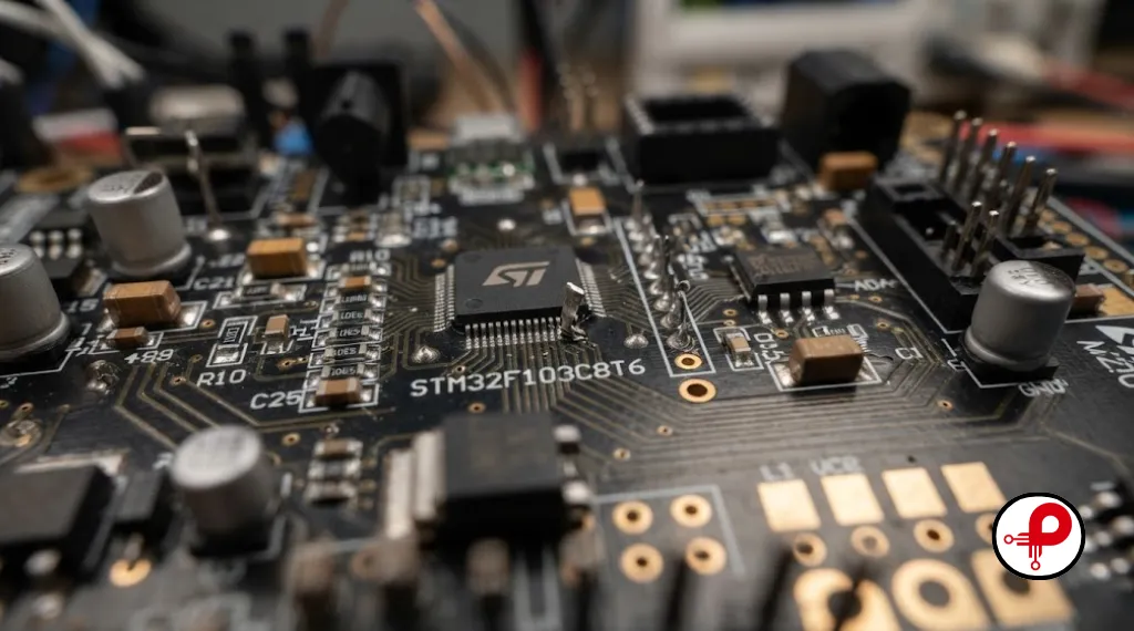
Even experienced engineers fall into these traps, and I have personally made most of them at some point.
1. Ignoring parasitic effects
Treating every trace as an ideal wire instead of accounting for parasitic inductance and capacitance at higher frequencies.
2. Poor grounding strategy
Splitting ground planes without a clear, single stitching point, which can create ground loops instead of preventing them.
3. Skipping simulation
Jumping straight to layout without simulating critical analog stages first.
4. Underestimating power integrity
Assuming a single decoupling capacitor per IC is enough without checking the actual current transients involved.
5. Late thermal analysis
Only checking thermal performance after the board is built rather than during layout, when component placement can still be adjusted.
6. Overlooking manufacturing tolerances
Designing a circuit that only works with the exact typical values from a datasheet, rather than the full tolerance range.
7. Weak documentation
Leaving no design notes, which turns even a working board into a maintenance headache six months later.
8. Not planning for testability
Failing to add test points for key signals, making debugging and production testing far harder than it needs to be.
Best Practices Checklist
Use this list as a quick reference before you commit a board to fabrication.
Design Review & Readiness Checklist
Design Tools and Software
Choosing the right tools makes a meaningful difference in both design speed and design quality.
| Tool Category | Common Use | Examples |
|---|---|---|
| Schematic capture and PCB layout | Circuit design and board layout | Altium Designer, KiCad, Eagle |
| Analog simulation | SPICE level circuit verification | LTspice, PSpice, Cadence Spectre |
| Digital simulation | RTL and gate level verification | ModelSim, Vivado Simulator |
| Hardware description languages | Digital logic design for FPGA and ASIC | Verilog, VHDL, SystemVerilog |
| Signal integrity analysis | High speed digital and RF verification | Ansys, Keysight ADS |
| Embedded development | Firmware for microcontrollers | Arduino IDE, STM32CubeIDE |
For teams working on connected products, setting up a development environment such as configuring the ESP32 for Arduino IDE is often one of the first practical steps once the hardware design reaches the prototype stage, since it lets firmware development start in parallel with board bring-up.
Challenges in Analog and Digital Circuit Design
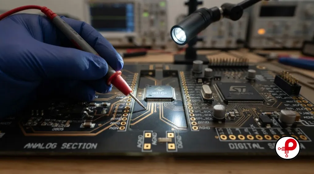
Analog and digital circuit design continues to become more challenging as electronic systems grow faster, smaller, and more complex. While modern design software has improved simulation and verification, engineers still face issues such as signal integrity, power integrity, electromagnetic interference (EMI), thermal management, and high speed PCB routing. Successfully addressing these challenges requires careful planning, proper component selection, and a well optimized PCB layout to ensure reliable and long lasting product performance.
Lower supply voltages leave less headroom for analog signal swing, making low noise analog design more demanding at newer process nodes.
Faster clock speeds push more digital designs into signal integrity territory that used to only matter for RF engineers.
Supply chain pressures force frequent redesigns around available parts, remaining a leading factor behind hardware startup failures.
Electromagnetic compatibility requirements demand proactive layout strategies from day one rather than treatment as a final test.
With fewer specialists focusing on analog compared to digital, experienced analog engineering talent is increasingly scarce and difficult to retain.
Frequently Asked Questions
1. What is analog and digital circuit design?
↑2. What is the difference between analog and digital circuit design?
↓3. How do analog and digital circuits work?
↓4. Which is better, analog or digital circuit design?
↓5. What is mixed signal circuit design?
↓6. What software is used for circuit design?
↓7. Do I need to learn both analog and digital design?
↓8. Is analog circuit design becoming obsolete?
↓Conclusion
Analog and digital circuit design are not competing disciplines, they are two halves of the same job. Every product that senses, measures, or interacts with the physical world needs analog circuitry, and nearly every product that computes, stores, or communicates data needs digital circuitry. The engineers who understand both, and who understand how to combine them cleanly on a real PCB, are the ones who consistently ship products that work the first time.
If you are starting a new hardware project and want an experienced team to handle everything from schematic capture through mixed signal PCB layout and validation, our engineers bring hands on experience across PCB design services, electronic hardware design, and embedded systems development. Reach out to discuss your project, and let’s figure out the right architecture for your product before you commit to a single line on a schematic.