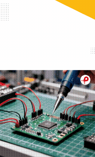


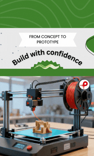

1. Starting Point for PCB Design
Among the most basic and vital fields in contemporary electronic engineering is PCB Design. Every electronic device you use every day—smartphone, laptop, smartwatch, medical equipment, or automotive control unit—relies on a well constructed Printed Circuit Board (PCB). Electronic components would stay separated and unable to work as a whole system without PCB Design.
Advances in artificial intelligence-assisted routing, automated design rule checking, cloud-based collaboration, and simulation programs have greatly changed PCB Design in 2026. These advances have accelerated PCB creation and made it more effective than ever before. Still, the fundamental ideas of PCB Design are still essential for engineers and beginners to fully comprehend despite technical advancement.
PCB Design goes beyond simply joining parts on a board. It is about designing a trustworthy, effective, and manufacturable system guaranteeing suitable electrical performance, thermal stability, and signal integrity. A well-designed PCB improves product life, lowers manufacturing costs, and guarantees steady functioning under actual circumstances. From fundamental ideas to sophisticated industry-level knowledge of PCB Design, this handbook offers a thorough systematic learning path.
2. PCB Design: What is it?

The engineering technique of turning an electronic circuit diagram into a physical layout suitable for production and use in actual electronic equipment is PCB Design. Arranging components on a board and connecting them with copper traces that let electrical signals go between various system components is called it.
PCB Design essentially builds a bridge between an electronic concept and a real hardware product. Even a flawlessly accurate circuit schematic cannot work in actual situations without good PCB design.
3. Significance of PCB Design in Electronics
Performance, dependability, and cost effectiveness of any electronic device depend greatly on PCB Design. A well-optimised PCB guarantees accurate power distribution throughout the system, less noise interference, and clear signal transmission.
Best Practices for Reliable PCB Design
The difference between a board that works and one that works reliably often comes down to the design decisions made before a single trace is routed. These core practices help engineers build PCBs that hold up in the real world — not just on the bench.
- Think about signal integrity before you start routing: Noisy or degraded signals are one of the most common causes of mysterious failures in electronic products. Getting your impedance, trace lengths, and return paths right from the beginning saves you from chasing ghosts later — and keeps your device communicating cleanly even under demanding conditions.
- Take heat seriously during layout, not after: Electronics generate heat, and heat degrades components over time. Building proper thermal relief into your design — through copper pours, thoughtful component spacing, and designated heat paths — keeps temperatures in check and adds real years to your product’s life.
- Don’t cut corners to save time in layout: It’s tempting to rush through the design phase, especially under deadline pressure. But shortcuts in PCB layout have a way of showing up at the worst possible moment — as short circuits, intermittent faults, or field failures. Doing it right the first time is almost always faster than fixing it after the boards come back.
- Design for how the product will actually be used: A PCB that looks good in simulation but falls apart under real operating conditions isn’t a finished design — it’s a starting point. Stable voltage rails, clean routing, and solid grounding all contribute to a product that behaves predictably whether it’s sitting on a desk or running in a demanding environment.
Particularly in sectors like automobile electronics, aviation systems, IoT devices, robotics, and medical equipment—where even small design mistakes can cause serious failures or safety risks—PCB Design is crucial. If you are working on early-stage products, you may also find our guide on [How to Reduce Your Prototype Cost Without Sacrificing Quality] helpful.
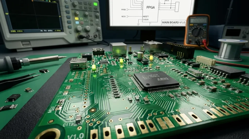
4. Board Layering and Layout
Multiple layers make up a Printed Circuit Board, each meant for a particular functional use in the general architecture.
Mechanical strength is provided by the base substrate, which also supports all electronic components. The copper layer transmits electrical messages between parts. By shielding copper traces from oxidation and avoiding short circuits, the solder mask layer serves protection. Components labeling and visual reference during assembly depend on the silkscreen layer.
Multiple interior layers are included in sophisticated PCB Design to manage intricate routing, power distribution, and high-speed signal transit. Due to their small size and great efficiency, multi-layer PCBs—which are increasingly used in current electronics—are also known as.
Typical PCB Layers Explained
The substrate — your board’s physical backbone
Every PCB starts with a base material, most commonly FR4 fiberglass, that gives the board its physical form. It holds everything in place and keeps the board from flexing, cracking, or failing when exposed to heat, vibration, or everyday handling.
Copper layers — where electricity actually travels
Thin sheets of copper laminated onto the substrate form the conductive paths that connect every component on your board. How these traces are routed — their width, spacing, and direction — directly determines how well your circuit performs and how much noise it generates.
Solder mask — the green coat doing quiet important work
That familiar green (or sometimes red, blue, or black) coating isn’t just for looks. It keeps solder exactly where it belongs during assembly, stops copper traces from oxidizing over time, and prevents accidental shorts between closely spaced pads — all of which matter a lot once your board is in the field.
Silkscreen — the layer that makes assembly human-friendly
Component labels, pin markers, polarity indicators, and board revision numbers all live on the silkscreen layer. It doesn’t affect how the circuit works, but anyone who’s tried to debug an unlabeled board knows exactly how much this layer matters when something goes wrong.
Internal layers — reserved for complex, high-speed designs
When a two-layer board can’t handle the routing complexity or signal demands of a design, engineers add internal copper layers dedicated to power planes and high-speed signal routing. These buried layers clean up power distribution, reduce electromagnetic interference, and make it possible to build the kind of dense, fast boards that modern electronics demand.
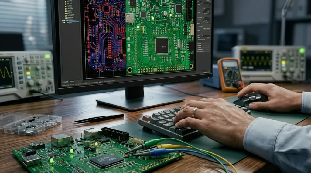
5. Procedures and PCB Design Workflow
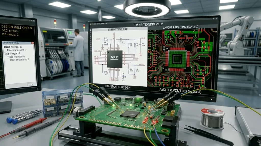
PCB Design uses a methodical engineering process that guarantees reliability and accuracy from idea to manufacturing.
Starting with schematic design, which sets out the electrical logic of the circuit, the process starts. Engineers next choose components according on cost, availability, and electrical needs.
PCB layout design follows next, wherein components are deliberately positioned to maximize performance and minimize interference. Following placement, routing ensures that all components are linked using copper traces while preserving signal integrity and spacing rules using professional PCB design tools such as [KiCad PCB design softwhttps://www.kicad.org/are]
The final stages comprise design rule checks (DRC), manufacturing file creation, and prototype testing to verify actual performance.
The PCB Design process comprises:
This step defines how components connect logically, forming the complete electrical blueprint of the circuit before physical design begins.
Components are selected based on performance, availability, and cost to ensure reliable and practical circuit operation.
Components are placed on the board strategically to ensure proper function, heat control, and efficient assembly.
Electrical connections are carefully routed to reduce noise, maintain signal quality, and improve circuit performance.
Design rules are checked to ensure the PCB meets manufacturing standards and avoids costly production errors.
Production files like Gerbers and drill data are created for accurate PCB fabrication.
Prototype boards are tested in real conditions to confirm performance before mass production.
Every phase depends on the one before it, hence accuracy is crucial at every stage.
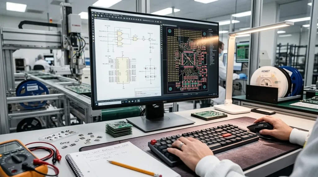
6. Programms and Tools for PCBs
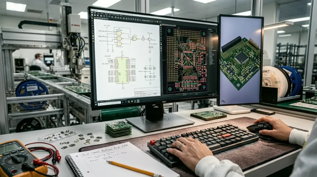
Specialized software tools used in PCB Design allow engineers to quickly create, simulate, and check circuits.
Because of their sophisticated capabilities and excellent accuracy, professional tools like Altium Designer, OrCAD, and Autodesk Eagle are extensively utilized in industrial and commercial contexts.
For novices, free tools like KiCad and EasyEDA are strongly advised as they provide full PCB Design functionality free of charge and are simple to pick up.
Modern PCB design technologies have capabilities including artificial intelligence-aided routing, real-time simulation, and cloud-based teamwork, all of which greatly boost design accuracy and productivity.
Among widely used tools are:
| Software | Best Suited For | What Makes It Worth Using |
|---|---|---|
| Altium Designer | Professional & enterprise teams | The go-to choice for complex, high-speed designs where simulation accuracy and clean manufacturing handoff aren’t optional. |
| KiCad | Independent designers & startups | Surprisingly capable for a free tool — handles real professional work and keeps improving thanks to a strong open-source community. |
| EasyEDA | Quick prototypes & remote teams | Browser-based and beginner-friendly, with direct links to component suppliers and PCB fabs that make ordering fast and simple. |
| Autodesk Eagle | Beginners & small-scale projects | A solid starting point for hobbyists — easy to learn, well-documented, and backed by years of community tutorials and resources. |
7. PCB Design Best Practices
One of the most important steps in guaranteeing performance and dependability of electronic systems is PCB layout design.
Engineers should concentrate on lowering signal path length, keeping appropriate grounding, and isolating analog and digital components to prevent interference.
Other critical techniques include arranging decoupling capacitors close to ICs, optimizing thermal distribution, and staying clear of sharp track angles that could cause signal degradation.
Best PCB Design Practices for Reliable Performance
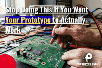
8. General PCB Design Errors
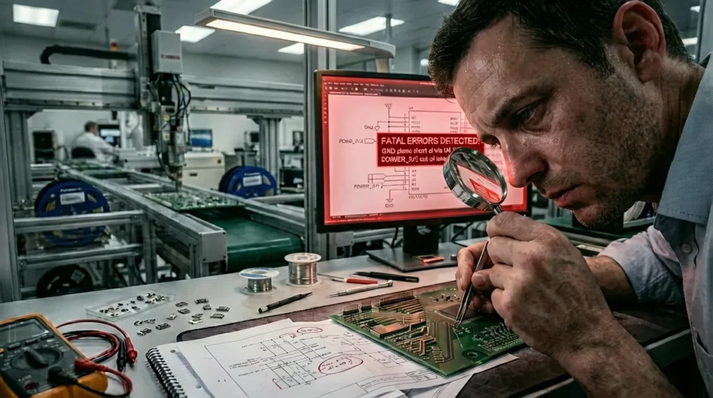
Most beginners make PCB mistakes that are completely avoidable — and unfortunately, they tend to show up at the worst possible time, like after the boards come back from fabrication. The usual culprits are grounding done wrong, components placed without thinking about how they’ll interact, and trace widths that simply can’t handle the current or signal speeds the circuit demands. Skipping design rule checks is another habit that catches up with you fast — problems that take five minutes to fix in software can mean days of delays and a full redesign once you’re holding a physical board.
Thermal management and signal integrity trip up a lot of new designers too. Ignore them and you get boards that overheat, behave unpredictably, or just stop working once they’re outside a controlled environment. The gap between a board that technically works and one that works reliably comes down to getting these fundamentals right every single time.
9. Online Free PCB Design Tools
Free instruments already on the market make PCB Design simple to learn.
KiCad and EasyEDA are extensively used as they enable full design processes including schematics creation, PCB layout, and manufacturing file generation.
Moreover allowing cloud-based access, teamwork, and project sharing without installing are several online PCB Design tools.
Among the benefits are:
- No mounting necessary
- Help with cloud storage
- Real-time cooperation
- Beginning learners have an easy learning curve
10. Sophisticated PCB Design Ideas
Advanced PCB design is all about using smart engineering techniques to make electronic systems faster, more stable, and more reliable in real-world conditions. In high-performance devices, engineers don’t just focus on basic connectivity—they carefully optimize multilayer boards, manage impedance, control EMI/EMC issues, and design clean high-speed signal paths. For more complex applications, they also work on power distribution networks and thermal simulations to ensure the system runs efficiently without overheating or signal degradation. These advanced methods are especially important in IoT devices, communication systems, and industrial-grade electronics where reliability is critical.
Multi-layer PCB optimization
Improves performance by efficiently stacking and organizing layers for better signal flow, reduced noise, and compact design.
Impedance matching
Ensures signal consistency by balancing electrical resistance in high-speed circuits, reducing reflection and data loss.
EMI/EMC control and high-speed routing
Minimizes electromagnetic interference while maintaining clean, stable signal paths in fast digital systems.
Power distribution and thermal simulation
Enhances system reliability by ensuring stable power delivery and preventing overheating through advanced thermal analysis.
11. PCB Fabrication, Applications, Career Path
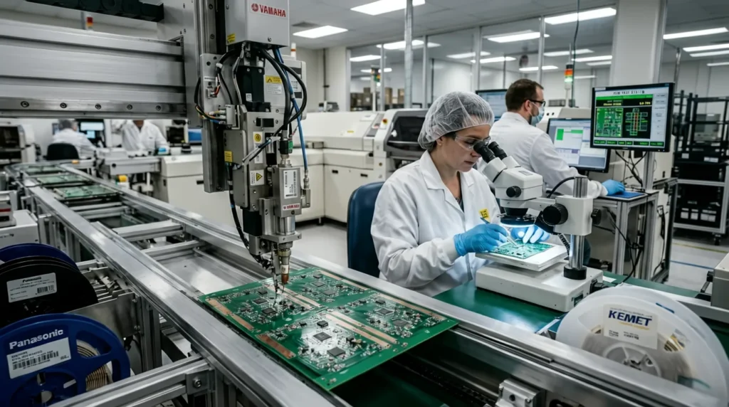
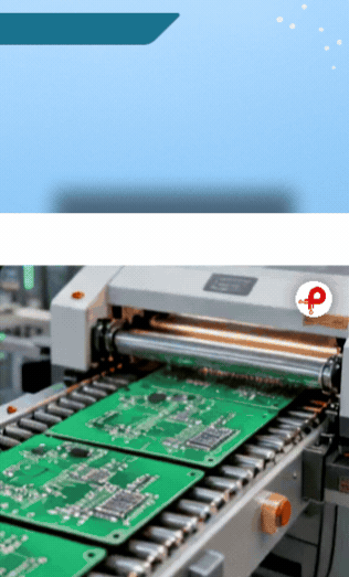
Once the design is finalized and verified, the manufacturing process takes over — moving from raw materials through fabrication, etching, drilling, solder mask application, and full component assembly to produce a finished, functional board.
PCB design sits at the heart of nearly every modern industry. From consumer electronics and automotive systems to medical devices, industrial automation, and IoT hardware, almost every technology sector depends on well-engineered circuit boards to power its products.
It’s also a field with strong and growing career demand. Engineers with serious PCB design skills are sought after across a range of roles — PCB Design Engineer, Hardware Engineer, Embedded Systems Engineer, and IoT Developer among them — with opportunities expanding as electronics become more deeply embedded in every industry.
For engineers willing to develop genuine expertise, PCB design opens doors to meaningful work, competitive salaries, and the satisfaction of seeing designs they built running inside real products people actually use.
12. Summary
Among the most crucial engineering abilities in 2026 is PCB Design. It serves as the foundation of all contemporary electronic devices and is critical for innovation and product development.
Modern tools, organized learning, and solid basics enable anybody to master PCB Design and go from novice level to professional engineering ability. This ability enables opportunities in industries including sophisticated hardware development, robotics, Internet of Things (IoT), and electronicsGet