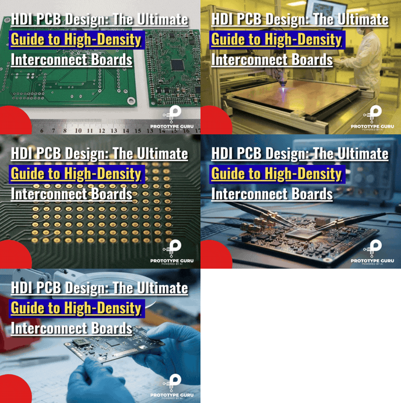









HDI PCB design is the practice of laying out printed circuit boards with far more connections per square centimetre than a conventional board allows. It does this with laser-drilled microvias, blind and buried vias, fine traces under 100 µm, and thin build-up layers added in sequential laminations. The result is a smaller, lighter board with shorter signal paths — the reason every modern smartphone, smartwatch, and high-speed compute module runs on HDI.
But HDI is not just “a normal PCB with smaller features.” Shrinking vias and traces changes the stack-up, the materials, the reliability risks, and the cost model. A layout that ignores these limits can pass DRC in your CAD tool and still fail at the fabricator — or worse, fail in the field after a few hundred thermal cycles.
This guide walks through HDI PCB design from the ground up: how IPC defines an HDI board, how microvias work, how HDI boards are actually manufactured, how to choose a stack-up, which design rules matter, how to keep signals clean, and how to avoid the microvia reliability traps that catch even experienced designers. If vias in general are new to you, start with our PCB Via Design Guide first, then come back here.
What Makes a PCB an HDI PCB?

IPC-2226, the sectional design standard for HDI boards, defines HDI simply as a board with higher wiring density per unit area than a conventional PCB. That definition is deliberately broad, so in practice fabricators use concrete markers: microvias instead of (or alongside) mechanically drilled vias, lines and spaces at or below about 100 µm, and pad densities of around 20 connections per cm² (NCAB Group).
If your board has even one layer of laser-drilled microvias, most fabricators will quote and process it as HDI. That single decision moves your board onto a different production line, with different equipment, different lead times, and different pricing.
The standards you will meet on an HDI project are:
- IPC-2226 – design rules and HDI construction types
- IPC-6012 – qualification and acceptance of rigid boards, including microvia structure and reliability
- IPC-4104 – dielectric and conductive materials for HDI build-up layers
- IPC-4101 – base laminate specifications
- IPC-4761 – via protection types (tented, plugged, filled, capped)
You do not need to memorise these documents, but you should know which one answers which question. Design questions go to IPC-2226; “will the fab accept this?” questions go to IPC-6012.
HDI PCB vs Standard PCB
| Feature | Standard PCB | HDI PCB |
|---|---|---|
| Via formation | Mechanical drill | Laser-drilled microvias + mechanical |
| Typical via diameter | 0.2–0.3 mm drill or larger | 75–150 µm (Ultra HDI below 75 µm) |
| Via aspect ratio | Up to ~10:1 (fab dependent, higher possible) | ≤1:1, ideally ~0.8:1 |
| Trace width / spacing | 100–150 µm and up | 75–100 µm, down to ~50 µm |
| Via types | Through-hole, some blind/buried | Microvia, blind, buried, stacked, staggered, via-in-pad |
| Lamination | Single press cycle | Sequential build-up (multiple cycles) |
| BGA pitch supported | ≥0.8 mm comfortably | 0.5 mm, 0.4 mm and below |
| Relative cost | Baseline | Higher; rises with each build-up layer |
These numbers are typical, not universal. Always confirm them against your fabricator’s capability sheet before you lock the stack-up.
Benefits of HDI PCBs
- Smaller form factor – the same circuit fits on a board that can be 30–50% smaller.
- Fewer layers – better routing efficiency often removes two or more layers compared with a through-hole-only design.
- Better electrical performance – shorter interconnects, lower via inductance and no long via stubs.
- Support for modern packages – fine-pitch BGAs, chip-scale packages and wafer-level packages simply cannot be routed without HDI.
- Lighter weight – important for wearables, drones and aerospace.
Microvias, Blind Vias and Buried Vias: The Core of HDI

The microvia is the feature that makes HDI possible. IPC-2226A and IPC-T-50M define a microvia as a blind structure with a maximum aspect ratio of 1:1 and a total depth of no more than 0.25 mm, measured from the capture land to the target land (Altium documentation). Most fabricators aim for about 0.8:1, because copper plating is far more reliable in a shallow hole.
Because a microvia normally spans just one thin dielectric layer (often 40–80 µm), it can be laser-drilled at 75–150 µm diameter. That frees space for traces and pads that a mechanical via would have consumed. A mechanical via with a 0.3 mm drill and 0.6 mm pad blocks every layer it passes through; a microvia with a 0.1 mm hole and 0.25 mm pad blocks only two layers and uses a fraction of the area. For a refresher on via anatomy — drill, pad, annular ring — see the Via (electronics) entry on Wikipedia.
Via types used in HDI PCB design
| Via Type | Spans | How it is made | Typical use |
|---|---|---|---|
| Through-hole via | All layers | Mechanical drill | Power, ground, connectors, core interconnect |
| Blind via | Outer layer to an inner layer | Laser or controlled-depth drill | Escape routing from surface pads |
| Buried via | Inner layer to inner layer | Drilled in the core before build-up | Core interconnect without using surface area |
| Microvia | One build-up layer (≤1:1 AR) | Laser drill | BGA fanout, layer-to-layer HDI routing |
| Skip via | Two dielectric layers in one hole | Laser drill | Fewer process steps, but harder to plate |
| Via-in-pad (VIPPO) | Inside an SMD pad, filled and capped | Laser/mechanical + resin or copper fill + cap plating | 0.5 mm and finer BGA pads |
Stacked vs staggered microvias
When a signal must cross several build-up layers, you have two choices:
- Stacked microvias sit directly on top of each other in a vertical column. They save the most space but require each lower via to be copper-filled, and they are the structure most associated with reliability problems (covered in the reliability section below).
- Staggered microvias step sideways at each layer, connected by a short trace or pad. They use more area but are mechanically more robust and usually cheaper to build.
A safe default is to stagger wherever space allows, and to limit stacks to two levels unless your fabricator has qualified deeper stacks for your exact build. Many designers use stacked vias only directly under the finest-pitch BGA, where there is no room to step sideways, and stagger everywhere else.
Via-in-pad
Via-in-pad places the via directly inside a component pad. On fine-pitch BGAs it is often the only way to escape the inner rows. The via must be filled (non-conductive resin or copper) and plated over flat — IPC-4761 Type VII — otherwise solder wicks into the hole during reflow and the joint voids or starves. Specify it clearly in your fabrication notes, because it adds cost and an extra process step. Via-in-pad is also very useful for decoupling capacitors under a BGA, because it removes the inductance of a dog-bone trace.
How HDI PCBs Are Manufactured
Understanding the fabrication process explains most HDI design rules. An HDI board is not pressed all at once; it is built up in stages, a process called sequential build-up (SBU) or sequential lamination.
Core Fabrication
A conventional multilayer core is made first, with its inner layers imaged, etched, and laminated. Buried vias in the core are mechanically drilled and plated at this stage.
First Build-Up Layer
A thin dielectric (prepreg or resin-coated copper) and copper foil are laminated onto each side of the core.
Laser Drilling
UV or CO₂ lasers ablate microvias down to the target pads on the layer below.
Desmear and Metallisation
Resin residue is cleaned out, and the holes are plated with copper. Stacked vias are filled with electroplated copper at this step.
Imaging and Etching
The new outer layer is patterned and etched.
Repeat Build-Up
Steps 2 through 5 are repeated sequentially for each extra build-up layer required (e.g., 2+N+2, 3+N+3 configurations).
Final Drilling, Plating & Finishing
Through-holes are drilled, the board is final plated, and solder mask, surface finish, and silkscreen are applied.
Every repeat adds a lamination heat cycle, a new registration step, and another chance for misalignment. This is why each build-up layer adds significant cost and lead time, and why registration tolerance drives capture-pad size. It is also why material choice matters: a laminate that survives one press cycle comfortably may delaminate after four.
HDI Stack-Up Structures: 1+N+1, 2+N+2 and Any-Layer

The stack-up is the first real decision in HDI PCB design, because it fixes cost, lamination cycles and which via spans you can use. The notation describes the build: the number before and after “N” is the count of build-up (microvia) layers on each side of the core, and “N” is the core itself.
IPC-2226 HDI types
IPC-2226 groups constructions into three main types (NCAB Group):
| IPC type | Microvia layers per side | Blind vias | Buried vias | Notation |
|---|---|---|---|---|
| Type I | 1 | Yes | No | 1+N+1 |
| Type II | 1 | Yes | Yes | 1+N+1 |
| Type III | 2 or more | Yes | Yes | 2+N+2, 3+N+3 |
All three types still use plated through-holes alongside the microvias. Beyond Type III sits any-layer (or every-layer) HDI, where every layer is a build-up layer and microvias can connect any adjacent pair. This is the construction used in flagship smartphone mainboards.
Choosing the right structure
- 1+N+1 – the entry point. One microvia layer handles fanout of 0.65 mm and many 0.5 mm BGAs; the rest routes on the core with through-holes. Lowest HDI cost.
- 2+N+2 – needed when a 0.5 mm or 0.4 mm BGA has too many rows to escape on one build-up layer. Adds lamination cycles and usually stacked or staggered microvias.
- 3+N+3 and any-layer – for very dense, high-pin-count devices and extreme miniaturisation. Highest cost, longest lead time, and the tightest reliability controls.
The rule of thumb is simple: pick the lowest HDI type that lets your densest component escape, then route everything else on the core.
Stack-up tips
- Keep the build-up symmetric about the core to prevent bow and twist.
- Put a solid reference plane directly under each high-speed build-up signal layer.
- Use thin dielectrics (roughly 50–100 µm) on build-up layers so microvias stay within aspect ratio.
- Place power and ground plane pairs close together in the core for low-inductance power delivery.
- Agree the stack-up with your fabricator before layout — they will adjust dielectric thicknesses for impedance and their own laser process.
Materials for HDI PCBs
HDI materials must survive several lamination cycles and multiple reflows, and they must laser-drill cleanly. Ordinary FR-4 with a coarse glass weave can leave uneven microvia walls, so build-up layers often use thinner, more uniform dielectrics.
| Material | Where it is used | Why |
|---|---|---|
| High-Tg FR-4 (Tg ≥ 170 °C) | Core and build-up | Withstands repeated lamination and lead-free reflow with less z-axis expansion |
| Spread-glass / laser-drillable prepreg | Build-up layers | Flatter glass weave gives cleaner laser holes and more consistent impedance |
| Resin-coated copper (RCC) | Outer build-up layers | No glass at all, so laser drilling is fast and clean |
| Low-loss laminates (e.g. modified epoxy, PPE blends) | High-speed and RF layers | Lower Df keeps insertion loss down at multi-GHz data rates |
| Polyimide | Rigid-flex HDI | Flexibility and high temperature resistance |
When choosing a laminate, look at four numbers on the datasheet: Tg (glass transition temperature), Td (decomposition temperature), z-axis CTE, and Dk/Df at your operating frequency. Low z-axis CTE matters most for HDI, because z-axis expansion is what pulls microvias apart during reflow. Hybrid stack-ups — low-loss material only on high-speed layers and standard high-Tg FR-4 elsewhere — are a common way to control cost. Our Thermal Management PCB Design guide covers how heat interacts with material choice.
HDI Design Rules and Fine-Pitch BGA Fanout
In most HDI projects, one component sets every rule: the finest-pitch BGA. Its pitch decides your via technology, your trace and space, and how many build-up layers you need.
Starting-point HDI design rules
| Parameter | Typical HDI value | Notes |
|---|---|---|
| Microvia drill | 75–125 µm (3–5 mil) | Ultra HDI goes below 75 µm |
| Microvia capture pad | 200–300 µm (8–12 mil) | Smaller pads need better registration |
| Microvia aspect ratio | ≤ 1:1, target ~0.8:1 | Depth ÷ diameter |
| Trace / space (build-up layers) | 75/75 µm (3/3 mil), down to ~50/50 µm | Thinner copper allows finer lines |
| Build-up dielectric | ~50–100 µm | Sets microvia AR and impedance |
| Mechanical via (core) | 0.2–0.25 mm drill | Through-hole and buried vias |
Treat these as a starting point, not a specification. Copy your fabricator’s actual capability numbers into your CAD constraint manager before routing a single trace, and set separate rules for the BGA escape region and open routing areas.
Fanout strategy by BGA pitch
| BGA pitch | Fanout method | Via technology | Typical HDI level |
|---|---|---|---|
| 1.0 mm and above | Dog-bone | Standard through-hole | Usually no HDI |
| 0.8 mm | Dog-bone | Through-hole or microvia | Standard or 1+N+1 |
| 0.65 mm | Dog-bone or via-in-pad | Microvia preferred | 1+N+1 |
| 0.5 mm | Via-in-pad | Microvia | 1+N+1 to 2+N+2 |
| 0.4 mm and below | Via-in-pad only | Stacked or staggered microvias | 2+N+2 or any-layer |
Cadence notes that 0.5 mm pitch is roughly where HDI becomes necessary, and that a 0.5 mm pitch can be split into 250 µm via pads with 50 µm trace and space (Cadence). At 0.4 mm there is simply no room for a dog-bone via on the diagonal between pads, so via-in-pad becomes mandatory.
Fanout best practices
- Escape the outer rows first on the top layer, then drop inner rows through microvias to layer 2, layer 3 and so on.
- Fan out away from the BGA centre to preserve routing channels.
- Use non-solder-mask-defined (NSMD) pads on fine-pitch BGAs unless the part vendor recommends otherwise.
- Assign power and ground balls to short vias straight into planes, and save routing channels for signals.
- Keep fiducials near fine-pitch parts for accurate placement — see PCB Fiducial Design.
- Review the part’s pinout early; sometimes swapping a few signals with the IC vendor’s approval saves a whole build-up layer.
HDI is almost entirely a surface-mount technology. If you are weighing package choices, our SMT vs Through-Hole guide explains the trade-offs, and the Surface-mount technology article on Wikipedia gives useful background.
Signal Integrity, Impedance and Power Integrity in HDI

HDI helps signal integrity in one big way: shorter paths and tiny vias mean less stub length, lower via inductance and less reflection than through-hole vias with long unused barrels. But fine geometry also brings new problems that must be designed out.
Impedance control
Thin build-up dielectrics change the trace width needed for a given impedance. A 50 Ω microstrip over a 60 µm dielectric may need a trace near 100 µm wide — fine for HDI — but the fabricator must hold that width tightly, because a few microns of etch variation now shifts impedance noticeably. There is a built-in tension: a thinner dielectric gives an easier microvia aspect ratio but a narrower, harder-to-control trace, while a thicker one does the opposite.
- Calculate impedance with your fabricator’s field solver and actual material Dk, not datasheet nominal values.
- Specify impedance-controlled nets and tolerance (typically ±10%) on the fabrication drawing.
- Request impedance test coupons on the production panel.
Crosstalk and routing
Tighter spacing raises crosstalk. Keep a solid reference plane under every high-speed build-up layer, route adjacent signal layers orthogonally, and use the 3W spacing rule for critical nets wherever density allows. Match lengths on differential pairs and DDR byte lanes inside the BGA escape, not only outside it. Avoid routing high-speed signals across plane splits, which breaks the return path. Our Signal Integrity PCB Design guide goes deeper on these techniques.
Power integrity
Dense processors draw high transient current through very small vias. A single microvia carries limited current, so use arrays of microvias for power and ground connections, place decoupling capacitors directly on via-in-pad connections under the BGA where possible, and keep power/ground plane pairs closely spaced for low plane inductance. For regulator layout, see PCB DC-DC Converter Design and Power Supply Filtering Circuit Design.
Thermal management
Packing more power into less area raises heat density. Use copper-filled via arrays under hot components as thermal paths to inner planes, and do not rely on thin build-up layers to spread heat on their own. Lower operating temperature also extends microvia life, so thermal design and reliability go hand in hand. Remember to derate components for the higher local temperatures found on dense boards (Component Derating Guidelines).
Microvia Reliability: The Hidden Risk in HDI Design

Microvias can fail even when boards pass every inspection. In 2019, IPC issued an industry warning after OEM members reported microvia failures in high-profile hardware that had already passed bare-board fabrication, inspection and acceptance (IPC). The related white paper, IPC-WP-023, linked stacked microvia problems to a weak interface between the microvia target pad and the electrolytic copper fill.
What makes this dangerous is timing. These failures typically happen during reflow but are often latent — undetectable at room temperature — so a board can test good, ship, and then go open in the field (Electronic Design).
Why microvias fail
- Weak interface separation – the bond at the base of the microvia cracks away from the target pad. This is the dominant failure mode.
- Z-axis expansion – above Tg, the dielectric expands far more than copper, pulling the via column apart during each reflow.
- Stack height – each level of a stacked column adds strain, and failures concentrate in stacks of three or more.
- Poor fill or plating – voids or incomplete fill in a lower via weaken the landing for the via above.
Design rules that reduce risk
- Prefer staggered microvias over stacked; if you must stack, keep it to two levels where possible.
- Choose laminates with low z-axis CTE and high Tg and Td.
- Minimise the number of reflow and rework cycles the board must survive.
- Keep microvia aspect ratio near 0.8:1, not at the 1:1 limit.
- For Class 3 or high-reliability products, require performance testing — reflow simulation with IST or via-chain continuity coupons per IPC-TM-650 2.6.27 — not just microsections.
- Ask your fabricator for microvia qualification data for your exact stack-up.
Designing test access into dense boards also matters, since HDI leaves little room for probe points — see PCB Design for Testability.
Common HDI PCB Design Mistakes
- Choosing the stack-up after placement. The stack-up must come first; changing it later forces a re-route.
- Using generic design rules. Default CAD rules rarely match an HDI fabricator’s laser, plating and registration capability.
- Over-stacking microvias. Three- and four-level stacks used “because the tool allows it” are the classic latent-failure source.
- Forgetting via-in-pad fill notes. Unfilled vias in BGA pads cause solder voids and opens.
- Fine lines everywhere. Using 50 µm traces across the whole board lowers yield; use them only where the BGA demands.
- Ignoring copper balance. Uneven copper between layers causes warpage, which hurts BGA soldering.
HDI Design for Manufacturing (DFM) Checklist
Most HDI respins come from design decisions the fabricator could not build, not from circuit errors. Run through this list before you release Gerbers or ODB++.
HDI PCB Design & Fabrication Checklist
Cost vs density trade-offs
HDI cost is driven mostly by lamination cycles, laser-drill count and special processes, not by layer count alone.
| Cost driver | Effect on price | How to control it |
|---|---|---|
| Extra build-up layers (1+N+1 → 2+N+2) | Large increase per step | Use the lowest type your densest BGA allows |
| Stacked microvias | Higher than staggered (needs copper fill) | Stagger where space permits |
| Via-in-pad fill and cap | Adds process steps | Use only under fine-pitch pads that need it |
| Very fine trace/space (< 75 µm) | Lower yield, higher cost | Use fine lines only in the BGA escape region |
| Low-loss or special laminates | Material premium | Use hybrid stack-ups: low-loss only on high-speed layers |
A common win: an HDI board often needs fewer total layers than the equivalent through-hole design, so it can end up close in price — and much smaller.
Where HDI PCBs Are Used

- Smartphones and tablets – any-layer HDI mainboards carrying 0.35–0.4 mm pitch processors and memory
- Wearables and hearables – tiny rigid-flex HDI boards where every square millimetre counts; see Low Power Circuit Design
- Networking, servers and AI accelerators – high-pin-count BGAs and multi-gigabit SerDes channels
- Automotive ADAS and infotainment – radar modules and compute units that need density plus high reliability
- Aerospace and defence – weight-sensitive avionics with strict reliability qualification
- Medical devices – implantables, hearing aids and portable diagnostics
Industrial interface boards (for example RS485 designs) and surge-protected power stages (Surge Protection PCB Design) rarely need HDI. When no fine-pitch part forces it, a standard multilayer board is cheaper and more robust.
Frequently Asked Questions about HDI PCB Design
1. What is the difference between HDI and a standard PCB?
↑This lets HDI boards pack more components into a smaller board area. In practice, HDI boards are smaller, thinner, and lighter, with higher interconnect density and better signal performance.
2. When should I consider using HDI PCB technology?
↓Smartphones, tablets and compact medical or aerospace electronics commonly require HDI because standard vias won’t fit between pads. HDI is also used when reducing layer count/board size is important, even if cost per layer is higher.
3. What is the maximum aspect ratio for a microvia?
↓Any via longer than that (aspect >1:1) is outside the formal “microvia” spec and is avoided. For example, NCAB notes typical microvia depth ~60–80 µm with hole diameter 80–100 µm (≈0.8:1).
4. Are stacked microvias reliable?
↓Industry best practice is to limit stacked microvias to two layers; for three or more microvia layers, use a staggered (offset) approach to spread stress. In short, stacked microvias require stringent manufacturing controls and testing to ensure reliability.
5. Which IPC standards apply to HDI PCBs?
↓These standards define how HDI boards must be designed and tested. For example, NCAB lists IPC-2226 and IPC-6012 as core design/acceptance standards, and IPC-4104 for laminate materials.
6. Is HDI PCB technology more expensive?
↓For instance, a single HDI 6-layer board may replace a standard 8-layer design. Also, smaller boards save material and shipping cost. Thus, HDI has higher upfront manufacturing cost, but it often pays off in form-factor and performance.
7. What are blind and buried vias?
↓– Buried vias connect inner layers only (not visible from the outside). Using blind/buried vias (laser microvias) lets designers route signals internally without occupying outer-layer real estate, which is why HDI PCBs can have so much connectivity in limited area. (Both types require precise fabrication, and IPC classifies them under HDI standards.)
8. How many HDI build-up layers are typical?
↓At ~0.65 mm BGA pitch, a 1+N+1 build is often sufficient. Very fine-pitch designs (0.4–0.5 mm) may use multiple lamination cycles. Each build-up adds process steps (and cost), so designers start with the minimum required, increasing layers only for density or signal needs.
Conclusion
Good HDI PCB design starts with the densest component and works outward: its pitch sets the via technology, the via technology sets the stack-up, and the stack-up sets materials, impedance and cost. Keep microvias within aspect ratio, prefer staggered over stacked, choose low z-axis CTE materials, and agree everything with your fabricator before layout begins. Do that, and HDI gives you smaller, faster, lighter boards without the latent reliability failures that catch rushed designs.
References and Further Reading
- Printed circuit board – Wikipedia
- Via (electronics) – Wikipedia
- Surface-mount technology – Wikipedia
- IPC-2226A preview (ANSI webstore)
- IPC warning on microvia reliability
- NCAB Group – HDI design trends
- NCAB Group – HDI types
- Altium – Support for microvias
- Cadence – PCB fanout for 0.5 mm pitch BGA
- AdvancedPCB – HDI PCB guide
- AllPCB – HDI PCB and IPC standards
- AllPCB – HDI PCBs: performance and reliability
- PCB Unlimited – HDI PCBs
- TwistedTraces – Smart PCB design