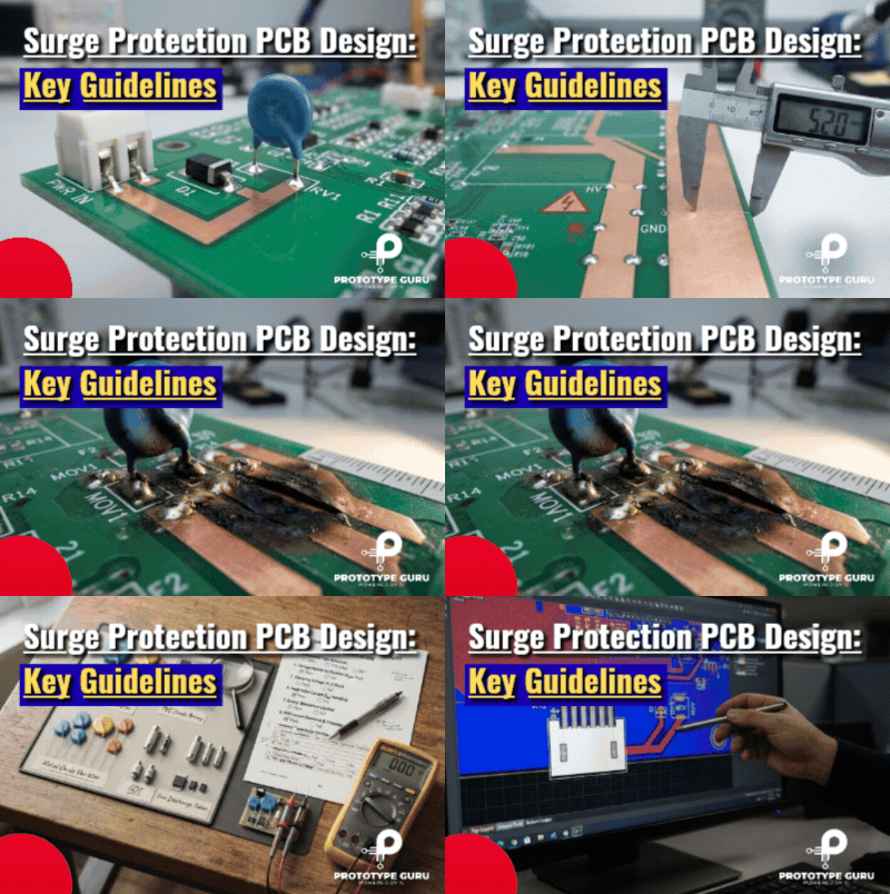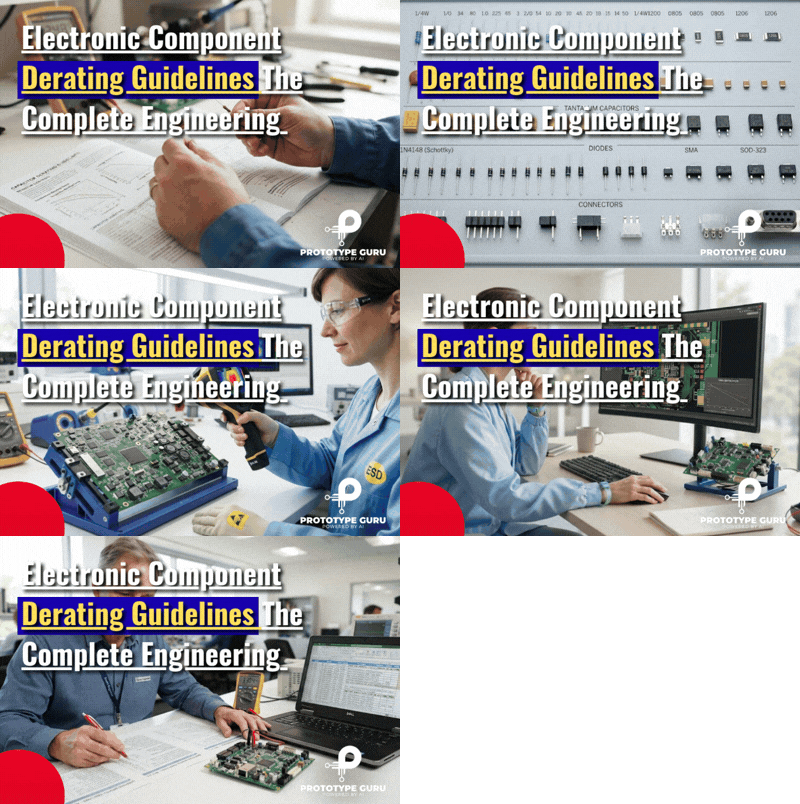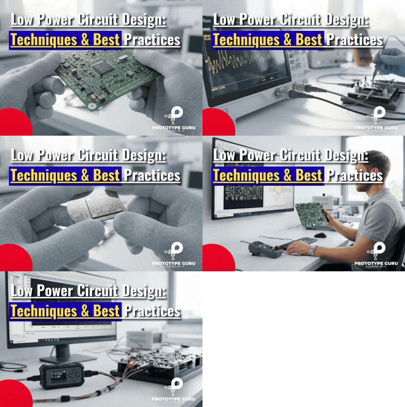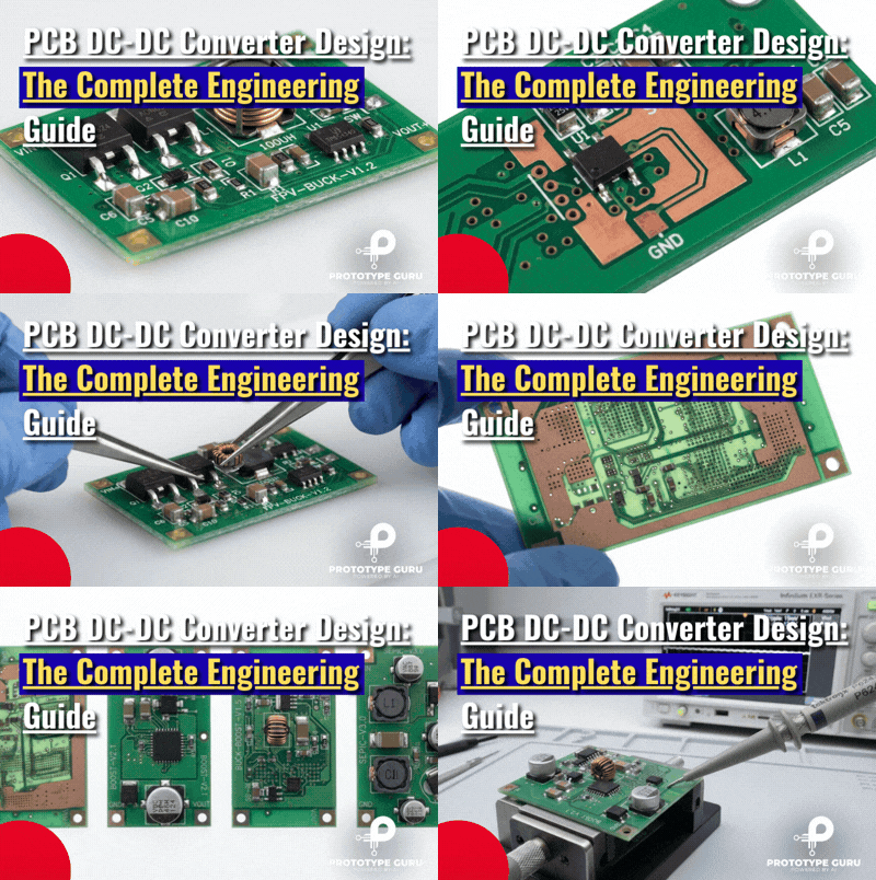









If you’ve ever built a converter that worked perfectly on the bench with dead-bug prototyping, then failed EMI testing or ran hot the moment it hit a real PCB, you already know the truth every power electronics engineer eventually learns: a PCB DC-DC converter is only as good as its layout. The schematic determines what the circuit is supposed to do. The PCB determines whether it actually does it.
I’ve spent the last eight years designing switching power stages for industrial controllers, wearables, and IoT hardware, and the single most common failure pattern I see, from junior engineers and experienced ones alike, is treating layout as an afterthought. This guide walks through everything that actually matters: topology selection, current loop control, grounding, thermal design, EMI mitigation, stackup, and the mistakes that quietly kill efficiency and reliability.
Quick answer: A PCB DC-DC converter is a switch-mode power supply built directly onto a printed circuit board, converting one DC voltage to another (step-down, step-up, or both) using an inductor, switching transistor(s), and capacitors. Layout quality, specifically minimizing high-frequency current loop area, is the dominant factor in efficiency, noise, and thermal performance, often mattering more than component selection alone.
1. What Is a PCB DC-DC Converter and Why Layout Wins the Design

A DC-DC converter PCB takes an input DC rail and produces a regulated output DC rail at a different voltage, using high-frequency switching rather than linear dissipation. That switching action is exactly what makes layout so critical: every time the switch node transitions, current has to change direction almost instantaneously somewhere on the board, and any parasitic inductance in that path shows up as ringing, overshoot, radiated noise, or lost efficiency.
Industry engineering notes are consistent on this point. Analog Devices’ own layout guidance for step-down regulators exists specifically because noise problems in switching supplies are almost always traced back to layout, not the schematic, and Texas Instruments frames PCB layout as a “critical portion of good power supply design” in its own regulator documentation, alongside a dedicated conducted-EMI application note for DC/DC converters.
In practical terms, this means:
Efficiency Variance
Two boards built from the identical schematic and BOM can have a 3 to 5% efficiency difference purely from layout.
EMI Compliance Failure
A converter that passes bench testing can still fail conducted or radiated EMI compliance because of a single oversized switch-node copper area.
Thermal Limitation
Thermal performance is often limited by copper geometry and via placement long before it’s limited by the silicon’s junction temperature rating.
If your team is scoping a new power stage, this is exactly the kind of decision that benefits from involving layout-aware engineers early. Our PCB design services team treats power section layout as a first-class design task, not a routing afterthought.
2. DC-DC Converter Topologies Compared: Buck, Boost, Buck-Boost, and SEPIC
Before laying out anything, you need the right topology. Each one has a distinct current path, and that current path is what dictates your layout strategy later.
| Topology | Voltage Relationship | Typical Efficiency | Best For | Layout Priority |
|---|---|---|---|---|
| Buck (step-down) | Vout < Vin | 90 to 98% | Point-of-load rails, battery step-down | Tight input capacitor loop |
| Boost (step-up) | Vout > Vin | 85 to 95% | Battery-powered boost to logic voltage | Tight output/diode loop |
| Buck-Boost | Vout above or below Vin | 80 to 92% | Wide input range, battery systems | Both input and output loops critical |
| SEPIC | Vout above or below Vin, non-inverting | 78 to 90% | Sensor nodes with variable battery input | Two inductors, larger footprint |
A buck converter has continuous current at the output and pulsating current at the input, so its input capacitor and high-side switch loop demand the most attention. A boost converter is the mirror image: continuous current at the input, pulsating current at the output, so the output capacitor and diode/switch loop become the priority. This is a distinction worth internalizing early, because it directly determines where you’ll spend your layout effort, engineering references on buck and boost PCB design consistently identify these as the two highest-noise loops in each topology.
Buck-boost and SEPIC converters combine both current profiles, which is why they tend to need more board area and more careful component grouping, you’re essentially managing two hot loops instead of one.
If your product needs to run from a single-cell battery down to near end-of-discharge voltage, buck-boost is usually the right call despite the lower efficiency, because it maintains regulation across the full battery discharge curve. For details on matching converter selection to a broader product architecture, our electronic hardware design engineers typically evaluate this trade-off during the requirements phase, not after a topology has already been locked in.
3. Core PCB Layout Principles: Current Loops and the Hot Loop

This is the section that separates a converter that meets spec from one that doesn’t. Every switching converter has what’s commonly called a “hot loop”, the path carrying the highest di/dt current, switching on and off at the converter’s switching frequency.
3.1 Identifying the Hot Loop
For a buck converter, the hot loop runs from the input capacitor, through the high-side switch, through the low-side switch (or diode), and back to the input capacitor’s ground return. Application guidance from Diodes Incorporated describes this loop plainly: it is the primary source of high-frequency noise in a switching converter, and it behaves like an antenna if left too large.
For a boost converter, the equivalent hot loop runs from the inductor, through the switch and diode, to the output capacitor, and back.
3.2 Minimizing Loop Area
The practical rule engineers apply on real boards:
- Place the input capacitor (buck) or output capacitor (boost) as physically close to the IC as the footprint allows, ideally on the same layer, with no vias in the critical path.
- Keep the switch node copper as small as physically possible; it only needs to be large enough to handle the current, not larger.
- Route the hot loop on a single layer where possible. Every via you add introduces additional parasitic inductance.
- Use multiple vias if the current must transition layers, rather than relying on a single via.
3.3 Separating Power and Signal
Feedback traces, compensation networks, and any analog sensing lines should be routed away from the switch node and the hot loop entirely. TI’s own layout comparisons between U-type and I-type multichannel buck layouts show measurable EMI differences purely from how the power loop geometry is arranged relative to sensitive nodes. This isn’t a minor stylistic choice; it’s a measured performance variable.
A practical checklist I use on every power stage review:
DC-DC Converter PCB Layout Checklist
Design Verification Steps
Teams that skip this stage often end up in a costly respin cycle. If you’re building a new power section and want it right the first time, it’s worth having it reviewed as part of a structured circuit board design process rather than discovering the loop problem during EMI pre-compliance testing.
4. Component Selection and Placement Guidelines

Layout and component selection are inseparable, the physical size, package, and parasitic characteristics of your parts determine how small you can realistically make the hot loop.
4.1 Inductor Selection
Choose a shielded inductor for noise-sensitive designs, as unshielded inductors radiate more electromagnetic interference into nearby traces. Size the inductor to achieve a ripple current of 20–40% of the maximum load current, balancing efficiency, cost, and performance, and always select an inductor with a saturation current rating that provides sufficient margin above the peak operating current rather than just the average current.
4.2 MOSFET / Switch Selection
Lower RDS(on) reduces conduction losses but often increases gate charge, leading to higher switching losses, so MOSFET selection requires balancing both factors rather than simply choosing the lowest RDS(on) value. In synchronous designs, the high-side and low-side FETs should be matched to the converter’s duty cycle, as a low-duty-cycle buck converter spends more time conducting through the low-side FET, making its losses more significant. Package selection is equally important, since thermal performance depends on the package design, with exposed-pad packages requiring a properly designed thermal via array underneath for effective heat dissipation.
4.3 Capacitor Selection
Use low-ESR ceramic capacitors for the high-frequency bypass directly at the switching IC to provide immediate charge and minimize high-frequency voltage ripples during fast switching transitions.
Add bulk capacitance, such as electrolytic or polymer types, further out on the rail to handle larger load transients, while keeping it physically separate from the strict high-frequency ceramic placement requirement near the IC.
Always derate ceramic capacitors for DC bias effects; a 10 µF-rated capacitor can lose 50% or more of its effective capacitance at rated operating voltage depending on the specific dielectric material used.
4.4 Component Placement Order
Engineers who route these boards well tend to follow a consistent sequence: place the switching IC first, then the input capacitor immediately beside its input pins, then the inductor, then the output capacitor, then the feedback divider, in that priority order, because each subsequent component has progressively more placement flexibility. This mirrors guidance published by regulator vendors describing the input capacitor as the single most placement-critical component in a step-down design.
If component sourcing and footprint decisions are proving to be a bottleneck, our electronic component selection resource covers how to balance parametric requirements against availability and cost without compromising layout intent, a common issue when a “drop-in equivalent” part turns out to have a different pinout or thermal pad geometry.
5. Grounding, Copper Pour, and Plane Strategy

Grounding mistakes are the single most common root cause of “unexplained” noise complaints I get asked to debug.
5.1 Solid Ground Plane vs. Split Planes
A single, continuous ground plane under the power stage is almost always preferable to splitting analog and power ground with a slot or moat. Crossing a split plane with a return current path creates a much larger loop than an uninterrupted plane, which increases both EMI and impedance. Guidance from PCB layout literature is explicit that crossing split planes is a common source of ground noise, and that stitching vias should connect any unavoidable split.
5.2 Copper Pour for Power Traces
Widen the power and ground traces well beyond the minimum PCB design rules to reduce voltage drop, improve current-carrying capability, and minimize heat generation. For high-current paths, use large copper pours instead of narrow traces whenever board space permits, as they provide lower resistance and better thermal performance. However, the switch-node copper pour is an important exception. Unlike other power nets, it should be kept as small as possible because excessive copper at the switch node increases parasitic capacitance, generates more electromagnetic interference (EMI), and can reduce the overall efficiency of the
5.3 Via Stitching
Stitching vias connect ground copper across layers, reduce loop inductance for return currents, and provide an additional thermal path. They’re inexpensive and there’s rarely a reason not to add generous stitching around the power stage perimeter, particularly near layer transitions and connector ground pins.
For antenna-adjacent or RF-coexistence designs, common in IoT products sharing a board with a DC-DC converter, grounding discipline becomes even more important, since switching noise can desensitize a nearby receiver. If your product includes wireless connectivity alongside power conversion, it’s worth reviewing our notes on [2.4 GHz PCB antenna design](https://prototypeguru.com/2 to 4-ghz-pcb-antenna-design/) to understand how converter placement relative to the antenna keeper-out zone affects RF performance.
6. Thermal Management Techniques for Power PCBs
Heat is the quiet failure mode. A converter can meet every electrical spec on the bench and still fail in the field because of thermal derating that nobody characterized.
6.1 Copper Thickness and Thermal Vias
Standard 1 oz copper is often insufficient for high-current power stages. Moving to 2 oz copper meaningfully reduces thermal resistance and improves current-carrying capacity without changing the schematic at all. For exposed-pad power components, an array of thermal vias directly under the pad, not offset to the side, is what actually transfers heat into internal copper layers.
6.2 Stackup for Heat Spreading
A four-or-more-layer board with a dedicated internal ground or power plane spreads heat far more effectively than a two-layer design, because that internal plane acts as a heat spreader across the entire board area rather than relying on surface copper alone.
6.3 Practical Thermal Checklist
DC-DC Converter Thermal Design Checklist
Verification Steps
6.4 Switching Frequency Trade-off
Higher switching frequencies shrink the inductor and capacitors, reducing board area and BOM cost, but they also increase switching losses, which directly worsens both thermal performance and EMI. For high-power designs, a lower frequency in the 100 to 300 kHz range is frequently the better trade-off; for compact, lower-power designs, 500 kHz and above is common. This is a decision to make deliberately, not by default settings in a reference design.
Products destined for enclosed housings, medical devices, industrial controllers, wearables, need this analysis done with the actual enclosure thermal path in mind. Our team has covered this in depth in the context of medical device development and wearable technology, where thermal budget is often the tightest constraint in the entire design.
7. EMI and EMC Design Practices
EMI failures are expensive precisely because they show up late, often at a compliance test house, after the board is already committed to tooling.
DC-DC Converter EMI & Noise Suppression Strategies
Where Converter EMI Comes From
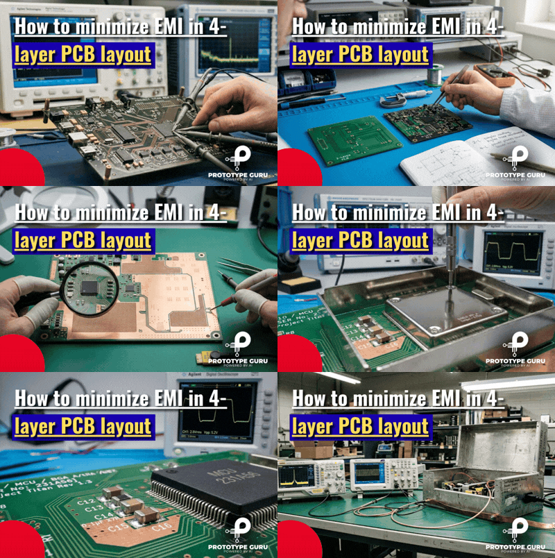
Conducted and radiated EMI in a DC-DC converter originate almost entirely from the hot loop’s di/dt and the switch node’s dv/dt. Reduce the physical area of both, and EMI drops correspondingly. This is the same principle applied specifically to compliance outcomes rather than just efficiency.
Filtering and Shielding
An input EMI filter, consisting of a common-mode choke and differential capacitors, is often necessary to meet conducted emissions limits, particularly in automotive or industrial products. Shielded inductors reduce radiated near-field coupling, while ground stitching around the power stage perimeter acts as a partial shield against radiated coupling.
Common EMI Mistakes
A pattern seen repeatedly: engineers fix a noise problem by adding a snubber or extra filtering after the fact, when the actual fix was a smaller switch node or a tighter hot loop that should have been designed in from the start. Snubbers and filters are legitimate tools, but they compensate for layout rather than replacing it.
Differential-Mode vs. Common-Mode Noise
Differential-mode noise travels through power and return conductors, addressed with capacitive filtering and loop reduction. Common-mode noise couples through parasitic capacitance to chassis or earth ground, typically needing a common-mode choke and careful grounding of the filter stage itself.
For products headed toward FCC, CE, or other regulatory certification, EMI performance isn’t optional polish, it’s a gating requirement. Our guide on how to certify an electronic product walks through what pre-compliance testing should look like before you commit to a production run.
8. Multilayer Stackup Recommendations
Layer count and stackup order directly affect noise coupling, current capacity, and cost.
| Layer Count | Typical Use Case | Notes |
|---|---|---|
| 2-layer | Low-power, cost-sensitive designs (<2A) | Requires careful pour and stitching to compensate for no internal ground plane |
| 4-layer | Most mainstream DC-DC converter PCBs | Dedicated ground plane on layer 2 dramatically improves EMI and thermal performance |
| 6-layer | High-current or mixed-signal boards | Allows separate power, ground, and signal layers with minimal coupling |
| 8+ layer | High-density, multi-rail, or EMI-critical designs | Used when multiple converters share a board with sensitive RF or analog sections |
A poor stackup choice, for example, sandwiching a small-signal layer directly between a high-current power layer and ground, increases capacitive noise coupling between layers, which is a documented failure pattern in switching regulator layout guidance. The better arrangement places the ground layer adjacent to the small-signal layer specifically to shield it.
If you’re deciding between a 2-layer and 4-layer board for a cost-sensitive product, the honest engineering answer is: 4-layer almost always pays for itself in reduced EMI rework and fewer respins, unless your current levels are genuinely low (well under 1A) and your EMI requirements are relaxed.
9. Common PCB Layout Mistakes and How to Fix Them
These are the mistakes I see most often in design review, roughly in order of frequency:
DC-DC Converter Common Layout Mistakes & Fixes
Oversized Switch Node Copper
Engineers sometimes widen the switch node trace or pour thinking it improves current handling. It usually just increases radiated EMI.
Fix: Size it only for the actual current, and no larger.
Input Capacitor Placed Too Far
Even a few extra millimeters of trace adds parasitic inductance to the hottest loop on the board.
Fix: Place the input capacitor first, before anything else, directly adjacent to the IC’s input and ground pins.
Feedback Trace Routed Near Noise
This couples switching noise directly into the control loop, causing instability or output ripple that looks like a compensation problem but is actually layout.
Fix: Route feedback traces away from noisy copper, and consider a local ground pour shield if space allows.
Relying on Autorouting for Power Stage
Autorouters optimize for connectivity, not for current loop area or parasitic inductance.
Fix: Route the power stage manually; autorouting is fine for low-current digital sections only.
Insufficient Thermal Vias
This is an easy one to miss because the board looks complete and passes DRC.
Fix: Check the datasheet’s recommended thermal via pattern explicitly; don’t assume the default footprint library part has it right.
Crossing Split Ground Plane
Crossing a split ground plane with a high-current return creates a large, uncontrolled loop and is a frequent EMI failure root cause.
Fix: Avoid ground splits under the power stage entirely, or stitch across them deliberately.
Ignoring Frequency Trade-offs
Defaulting to whatever frequency the reference design used, without evaluating your own size, thermal, and EMI constraints.
Fix: Treat switching frequency as a design variable, not a fixed default.
10. Quick Decision Guide: Topology and Layer Count

Use this as a fast starting point, then validate against your actual voltage range, current, and certification requirements:
- Need a single-direction step-down, fixed input range, currents under 3A? Buck converter, 2 or 4-layer board depending on EMI requirements.
- Need to step up from a single battery cell to a fixed logic rail? Boost converter, 4-layer board recommended for noise-sensitive loads.
- Input voltage crosses above and below the output voltage (e.g., wide battery discharge range)? Buck-boost, 4-layer minimum.
- Battery-powered sensor node with highly variable input and non-inverting output required? SEPIC, budget extra board area for two inductors.
- Currents above 5A or automotive/industrial thermal requirements? 4 to 6-layer board, 2 oz copper minimum, dedicated thermal via array.
- Board shares space with wireless radio or sensitive analog circuitry? Prioritize a solid ground plane and physical separation over cost savings on layer count.
This kind of framework is useful for early architecture decisions, but real products usually have constraints, enclosure size, certification region, cost target, that shift the answer. That’s the kind of trade-off analysis we walk clients through during product development scoping, before layout work even begins.
11. Testing, Validation, and Manufacturing Considerations

A converter design isn’t finished when the layout is routed, it’s finished when it’s been validated on real hardware and confirmed manufacturable at volume.
11.1 Bench Validation
Measure efficiency across the full load range rather than at a single typical operating point, as many converters perform well at 50% load but less efficiently near minimum or maximum load. Check the output ripple using the correct oscilloscope probing technique, such as a short ground spring instead of a long ground lead, because improper measurements can overstate ripple by two to three times. Finally, use thermal imaging while the board operates under sustained full load to identify hotspots that may not be visible during a brief bench test.
11.2 Pre-Compliance EMI Scanning
Running a pre-compliance conducted and radiated emissions scan before committing to production tooling catches the majority of EMI failures at a fraction of the cost of a failed formal compliance test. This is a step worth budgeting time and equipment access for, even on lower-volume products.
11.3 Design for Manufacturing (DFM) and Test (DFT)
Confirm that the thermal via sizes and tenting strategy do not cause solder wicking during reflow, especially for exposed-pad components. Add dedicated test points on critical nets such as Vin, Vout, feedback, and the switch node to simplify production testing without requiring access to fine-pitch IC pins. Finally, review the panelization and overall copper balance across the PCB panel, as large power-stage copper pours can lead to board warping if the copper distribution is uneven.
Getting DFM and test access right the first time avoids a painful cycle of board respins after the first production run. Our PCB testing and inspection process is built specifically to catch these issues before they reach volume manufacturing, and our PCB layout best practices resource covers additional DFM detail beyond what’s practical to include here.
If your product also includes embedded firmware controlling power sequencing or monitoring, common in IoT and industrial designs, coordinate the power-good and sequencing signals early with the embedded systems development team, since power-up ordering issues are notoriously difficult to debug after the board is already fabricated. For designs built around common connectivity platforms, our ESP32 selection guide also covers power rail requirements that interact directly with converter design choices.
Frequently Asked Questions
1. What is the most important layout rule for a DC-DC converter PCB?
↑2. How close should the input capacitor be to a buck converter IC?
↓3. Why does my converter have more output ripple than the datasheet suggests?
↓4. What causes EMI failures in switching converter designs?
↓5. Should I use an autorouter for a power supply PCB?
↓6. Why is my inductor getting hot?
↓7. Does copper thickness really matter for DC-DC converter PCBs?
↓8. What’s the biggest mistake new engineers make with DC-DC converter layout?
↓Related Services
If you’re scoping a new power-converter PCB or debugging an existing one, our team supports the full lifecycle: PCB design services, circuit board design rules review, electronic component selection, PCB testing and inspection, and full product development support from concept through certification. We’ve also written about why so many hardware startups fail at exactly this stage, underestimating the engineering depth a “simple” power stage actually requires.
If your DC-DC converter design is heading toward a compliance deadline, a thermal issue you can’t pin down, or a first-pass layout that needs an experienced second set of eyes, reach out to our engineering team before you commit to fabrication. A short design review at this stage is almost always cheaper than a respin after the boards come back.