









Most hardware startups do not fail because founders lack good ideas. They fail because the gap between a working prototype and a manufacturable, certifiable, sellable product is far wider than anyone expects. After spending years inside electronic product development, sitting through post-mortems, and helping teams rescue projects that had already burned through their seed round, I can tell you the pattern repeats itself with almost boring consistency.
If you are building a connected device, a wearable, an industrial sensor, or any physical product with electronics inside it, this guide walks through exactly why hardware startups fail and, more importantly, what a disciplined hardware product development process looks like when it actually works. This is not a theoretical article. It is built around the same PCB design, DFM, and certification decisions that separate the 10 percent of hardware startups that reach the market from the 90 percent that never do.
The Hardware Startup Reality Check

The numbers around hardware startups are sobering, and every founder should see them before writing a single line of a pitch deck.
Research from CB Insights identified lack of consumer demand as the number one reason hardware products failed, and its broader analysis of financing patterns showed how difficult it is for hardware companies to move past a single funding round, since prototyping alone can consume an entire seed budget. Industry data compiled by MacroFab paints an even starker picture: only around 24 percent of hardware startups manage to raise a second round of funding, and roughly 97 percent eventually shut down or stall out as inactive companies. Separate reporting pointing to the same MacroFab and CB Insights research puts hardware creation success rates well under 10 percent.
A more operational breakdown from industry analysts found that 42 percent of failed hardware startups pointed to overly long development timelines, while 34 percent cited a poor product market fit as the deciding factor. And a manufacturing-focused analysis from Hemar Group put a number on the post-prototype cliff: more than 70 percent of hardware startups never reach mass production, largely because the distance between a hand built demo and a certified, mass produced product is far bigger than founders assume.
| Failure Stage | Reported Failure Rate | Primary Driver |
|---|---|---|
| Idea to working prototype | Roughly 40 to 50 percent stall | Underestimated engineering scope |
| Prototype to mass production | Over 70 percent never reach it | Skipped DFM, certification, sourcing |
| First funding round to second round | Only about 24 percent raise again | Slow development, weak product market fit |
| Crowdfunded hardware products | Around 97 percent fail to fully deliver | Underestimated cost and manufacturing complexity |
Table sources: CB Insights hardware startup research, MacroFab analysis, RoboticsTomorrow, and Titoma industry reporting.
These are not reasons to avoid building hardware. They are reasons to treat hardware product development as an engineering discipline with a process, not a side project you figure out as you go.
Why Hardware Startups Fail: 11 Root Causes
Below are the recurring hardware startup mistakes I see across almost every failed or stalled project, followed by what actually fixes them.
-
1. Building Before Validating
Founders fall in love with a solution before confirming the problem. Skip the full electronics prototyping until you have talked to 30 to 50 target customers and validated your concept.
-
2. Underestimating Hardware Product Development Costs
Hardware is not software; it has non-zero marginal costs. Budget for at least three full PCB design/layout revisions and a 15 to 20 percent contingency on top of your engineering quote.
-
3. Skipping Design for Manufacturing (DFM)
A bench-top prototype is not ready for mass production. Bring a DFM review into your process before the design is frozen to avoid costly surprises in assembly and component tolerances.
-
4. Poor PCB Design and Layout Practices
Confusing schematic design with physical layout, or ignoring signal integrity, leads to field failures. Always run a formal design rule check against IPC standards before every design freeze.
-
5. Ignoring EMI, EMC, and Signal Integrity Early
Grounding mistakes and high-frequency noise are often invisible until compliance testing. Design your stack-up and grounding scheme with EMI/EMC in mind from the very first PCB pass.
-
6. No Certification Strategy
Treating FCC, CE, or wireless certifications as a final checkbox leads to expensive, last-minute redesigns. Design against your target compliance standards from day one.
-
7. Choosing the Wrong Manufacturing Partner
Never pick a manufacturer based solely on unit price. Evaluate partners on their quality systems, communication speed, and relevant experience with your specific product category.
-
8. Weak Supply Chain Management
Single-sourced parts and long lead times can stall production for months. Build bill of materials (BOM) risk assessment into your process and identify alternate parts for all critical components.
-
9. Underinvesting in Firmware and Embedded Software
Treat firmware with the same rigor as your physical hardware. Lack of dedicated test hardware and version control often leads to buggy launches and expensive post-release patches.
-
10. Hiring the Wrong Engineering Team
Hardware spans electrical, mechanical, and firmware disciplines. Avoid blind spots by building a cross-functional team or working with a partner capable of covering all three domains.
-
11. Running Out of Money
Financial failure is usually a downstream result of the mistakes above. Resolve your engineering, manufacturing, and validation processes early to ensure your cash runway lasts until launch.
The Hardware Product Development Process That Actually Works

A repeatable hardware product development process is the single biggest differentiator between startups that ship and startups that stall. Here is the sequence I recommend, and it mirrors the complete electronic product design workflow that experienced product teams follow.
- Problem validation and proof of concept. Confirm the technical approach works and the customer problem is real before investing in polished electronics prototyping.
- Minimum viable product (MVP). Build a functional MVP focused on the core value proposition, not every feature on your roadmap.
- Rapid prototyping. Move quickly through iterations. If your product involves connectivity, resources like how to build an IoT prototype quickly or how to make a Bluetooth device can shortcut months of trial and error.
- PCB design and PCB layout. Understand that these are two distinct disciplines. Our breakdown of PCB design vs PCB layout explains where schematic capture ends and physical layout begins.
- Design for manufacturing review. Validate component sourcing, assembly tolerances, and enclosure manufacturability before locking the design.
- Certification planning. Learn how to certify an electronic product and design against your target market’s standards from the beginning.
- Pilot production run. Build a small batch through your intended manufacturing partner to catch assembly issues before committing to volume.
- Volume manufacturing. Scale up using a validated PCB manufacturing process and a proven PCB manufacturing and assembly process.
Startups that compress or skip steps in this sequence are the ones that show up in the failure statistics above. Startups that respect the sequence, even under time pressure, are the ones that make it to shelf.
PCB Design Fundamentals Every Hardware Startup Must Know
Printed circuit board design is the technical backbone of almost every hardware product, and it is also where I see the most costly hardware startup mistakes originate. A handful of fundamentals deserve dedicated attention because they show up in nearly every design review.
1. IPC Standards
PCB design and manufacturing are governed by standards like the IPC-2221 series. These serve as the foundation for material selection, conductor spacing, and safety requirements. Designing without referencing these standards is one of the fastest ways to fail a manufacturability or safety review.
2. Trace Width
Trace width determines how much current a copper trace can safely carry without excessive heating. It is calculated based on copper weight, allowable temperature rise, and whether the trace is positioned on an internal or external layer.
3. Clearance and Creepage
Clearance is the shortest through-air distance between two conductors, while creepage is the distance along the surface of the insulating material. Both are voltage-dependent; ignoring these can create arcing risks or lead to safety certification failures.
4. Stack-up
Your layer stack-up defines how power, ground, and signal layers are arranged through the board thickness. A poorly planned stack-up is a primary root cause of EMI problems and signal integrity failures.
5. Grounding
A clean, low-impedance ground return path is the single most important factor in a reliable, EMI-quiet design. Split or fragmented ground planes are a recurring source of field failures.
6. Routing
High-speed and sensitive analog signals require controlled routing, appropriate spacing from noisy traces, and strict attention to return path continuity, rather than just connecting pins.
For a deeper technical walkthrough of these principles, our guides on circuit board design rules and PCB layout best practices go through real design examples, and our article on common PCB design mistakes catalogs the errors that most frequently trip up first time hardware teams.
EMI, EMC, and Signal Integrity: The Silent Product Killers

Electromagnetic interference, electromagnetic compatibility, and signal integrity problems rarely show up until a product is under real world conditions or sitting in a compliance test chamber, which is exactly why they are so dangerous for hardware startups on a tight timeline.
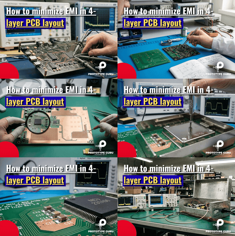
EMI issues typically stem from switching power supplies, fast digital edges, or antennas placed too close to noisy circuitry. Our detailed breakdown of EMI issues, causes, examples, and fixes walks through the most common failure patterns we see in the field. High frequency switching regulators deserve particular attention, since high frequency switching noise issues are one of the leading causes of failed EMC pre-compliance testing.
Once a design is close to final, formal electromagnetic compatibility testing should confirm the product meets the emissions and immunity limits required for your target market, well before you commit to a certification lab appointment for official approval.
Expert tip: Run informal pre-compliance EMI scanning in-house or with a low cost lab partner during your prototype phase. It is dramatically cheaper to fix a grounding or stack-up issue at prototype stage than after a failed formal certification test.
Custom PCB Design vs Off the Shelf Solutions
One of the earliest and most consequential decisions in hardware product development is whether to design a fully custom PCB or build around an off the shelf module or development board, such as an Arduino based platform. Our comparison of custom PCB design vs off the shelf solutions covers this in depth, but here is the short version.
| Factor | Off the Shelf Module or Dev Board | Custom PCB Design |
|---|---|---|
| Speed to first prototype | Fastest, often days | Slower, typically weeks |
| Unit cost at volume | Higher, module markup persists | Lower once tooled and optimized |
| Form factor control | Limited | Full control |
| Certification complexity | Sometimes inherits module certification | Requires full product-level certification |
| Long term scalability | Limited beyond low volume | Built for scale |
| Best fit | Early proof of concept | MVP through mass production |
A common and effective pattern is validating your idea on a dev board such as those covered in our Arduino Uno Q guide, then transitioning to a purpose built custom PCB once product market fit is confirmed. Startups that stay on a development board too long into production usually pay for it in unit cost and certification headaches later.
If you are inheriting or evaluating an existing board rather than starting from scratch, our guide to reverse engineering electronic circuits is a useful reference for understanding an unfamiliar design before you build on top of it. For teams building physical products beyond electronics, our overview of industrial product design engineering and our consumer electronics product design guide cover the mechanical and enclosure side of the equation.
Real Hardware Startup Failures and What They Teach Us

Looking at well documented hardware startup collapses is one of the fastest ways to internalize these lessons.
Jawbone. Despite raising roughly 930 million dollars over a decade, Jawbone was unable to hold onto meaningful market share for its headsets, fitness trackers, and speakers, and it shut down operations in 2017. CB Insights research ranks it among the costliest venture-backed startup failures on record. The lesson is that funding alone cannot substitute for sustainable product market fit and disciplined execution.
Juicero. Frequently cited alongside Jawbone in hardware startup post-mortems, Juicero built an elegantly engineered but massively overbuilt product that solved a problem consumers did not feel strongly enough to pay a premium for. It is the clearest example in recent hardware history of building before validating.
Pebble. An early crowdfunding success story, Pebble ultimately could not keep pace with better funded competitors entering the smartwatch category, illustrating how quickly a hardware lead can evaporate once larger players with deeper manufacturing and supply chain resources enter the same space.
The common thread across nearly every well known hardware startup failure is not a single catastrophic mistake. It is an accumulation of the eleven root causes covered earlier, compounding over 18 to 36 months until the runway simply runs out.
Hardware Startup Success Checklist
Use this as a working checklist before every major milestone.
Customer problem validated with real conversations, not assumptions.
Proof of concept confirms core technical feasibility.
MVP scope limited to the essential value proposition.
Engineering budget includes at least three PCB design and layout revisions.
DFM review completed before design freeze.
IPC standards referenced in your PCB design rules and stack-up.
EMI and signal integrity considered at layout stage, not after.
Certification strategy defined before final design lock.
Manufacturing partner vetted on quality systems, not just price.
Bill of materials includes alternate sourcing for critical components.
Firmware development treated as a first-class engineering discipline.
Cross-functional team covering electrical, mechanical, and firmware.
Contingency budget of at least 15 to 20 percent above the base quote.
Choosing the Right Manufacturing and Design Partner

Many first time hardware founders try to manage electrical engineering, mechanical design, firmware, DFM, and manufacturing coordination entirely in house, and then wonder why timelines slip. Experienced hardware design services and product engineering services partners exist precisely because these disciplines rarely live well inside a single small team without prior hardware experience.
When evaluating a partner, look for a track record across the full journey: proof of concept, PCB design and layout, embedded software, DFM, certification support, and PCB manufacturing and assembly coordination. A partner who only does layout work, or only does manufacturing, forces you to manage the seams yourself, and the seams are exactly where hardware startup mistakes tend to hide.
FAQ
1. Why do most hardware startups fail?
↑2. What percentage of hardware startups fail?
↓3. What is the biggest mistake in hardware product development?
↓4. How long does it take to bring a hardware product to market?
↓5. Should a hardware startup use a development board or design a custom PCB?
↓6. How much does hardware product development cost?
↓7. Why is Design for Manufacturing (DFM) important for hardware startups?
↓8. How can hardware startups improve their chances of success?
↓Final Thoughts
Hardware is hard, but it is not unpredictable. The startups that make it through to volume manufacturing are rarely the ones with the flashiest idea. They are the ones that treat proof of concept, PCB design, DFM, and certification as sequential, non-negotiable stages of a real hardware product development process, rather than steps to rush past on the way to a launch date.
If your team is navigating PCB design, DFM, or certification planning and wants a second set of experienced eyes before you commit to tooling, our engineering team works with hardware startups through every stage of this process, from proof of concept through certified production. Reach out to talk through where your product stands today and what the next milestone should look like.