










If you have ever sent a board to fabrication only to have it come back with shorted traces, failed impedance, or a rejection notice from your assembly house, you already know why circuit board design rules exist. After spending years reviewing layouts before they go to manufacturing, I can tell you that almost every board failure traces back to the same handful of overlooked rules: clearance, trace width, grounding, and stack-up.
This guide breaks down circuit board design rules the way a working engineer actually uses them, not as abstract theory, but as numbers you can type into your design rule checker today. We will cover basic PCB design rules, IPC PCB design rules, high-speed PCB design rules, and the specific requirements for analog, digital, mixed-signal, high-voltage, and high-frequency boards. You will also get comparison tables, a manufacturing checklist, and answers to the questions engineers search for most.
Whether you are a hobbyist laying out your first board in KiCad or a startup preparing a design for mass production, understanding circuit board design rules is what separates a board that works once on your bench from a product that ships reliably by the thousands. If you are still deciding between building an in-house layout and outsourcing it, our comparison of custom PCB design versus off-the-shelf solutions is worth reading first.
1. What Are Circuit Board Design Rules
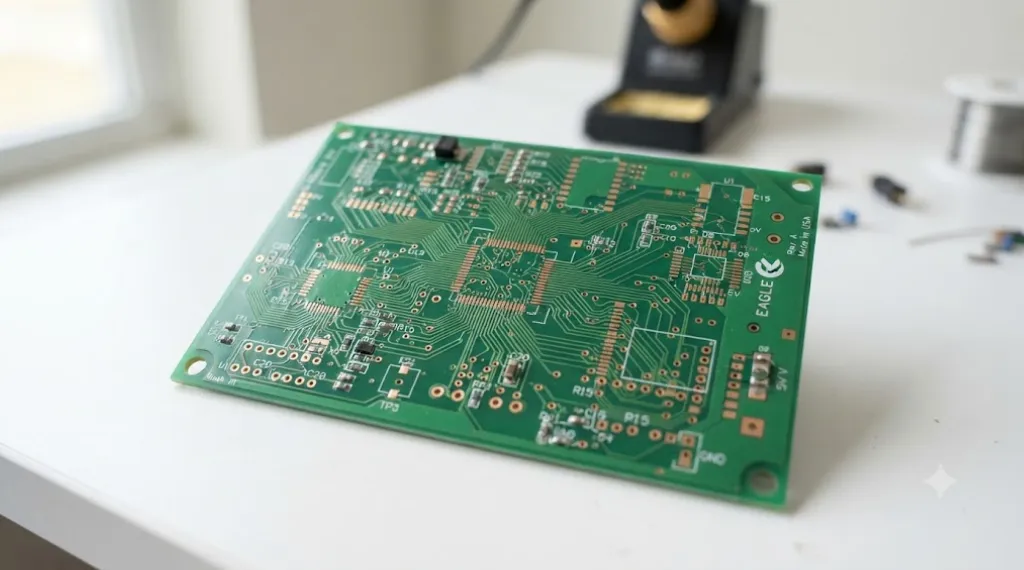
Circuit board design rules are the measurable constraints that define how close copper features can sit next to each other, how wide a trace must be to carry a given current, how large a drill hole and annular ring need to be, and how components should be placed and labeled. These rules are entered into your EDA software as a Design Rule Check, or DRC, so the software flags a violation before you ever send a file to a fabricator.
There are really two layers to this. Design standards, published by bodies like IPC, are industry-wide guidelines that apply broadly. Design rules are the specific values you enter into your PCB layout guidelines settings, often narrowed down by your chosen manufacturer’s actual production capabilities. A board that passes IPC-2221 in theory can still get rejected if it ignores your fabricator’s minimum trace and space capability, so both layers matter.
2. Why PCB Design Rules Matter
Skipping circuit board design rules is the single most common reason boards get delayed, respun, or fail in the field. A few consequences I have seen firsthand:
Manufacturing Rejections
Traces or spacing below your fabricator’s minimum trace and space capability cause the board house to hold your order or ask for a redesign.
Field Failures
Insufficient clearance under humid or high-altitude conditions leads to arcing, dendritic growth, and eventual short circuits months after shipment.
EMI and Compliance Failures
Poor stack-up and grounding push a product past regulatory emissions limits, forcing a redesign after certification testing has already been paid for.
Wasted Budget and Schedule
Every PCB design mistake caught after fabrication costs far more to fix than one caught during layout review. Our breakdown of the most frequent PCB design mistakes covers this in more depth.
Getting circuit board design rules right up front is cheaper than fixing them later, and it is the fastest way to move from prototype to a reliable production-ready product, a process we walk through in the Complete Electronic Product Design Workflow.
3. Basic PCB Design Rules Every Engineer Should Know
Before touching high-speed routing or impedance control, every layout needs to satisfy a set of basic PCB design rules. These apply regardless of whether you are building a simple two-layer board or a sixteen-layer server card.
Grid and outline. Set your placement grid before dropping a single part, typically 0.1 inch or 2.54 mm, since it aligns with most standard component footprints and keeps routing tidy. Draw a clean, simple board outline; unusual shapes should only be used when mechanically required, because odd outlines slow down panelization and increase fabrication cost.
Component placement. Group components by function, keep signal flow moving in one direction (inputs on one side, outputs on the other), and place decoupling capacitors as close as possible to IC power pins. Logical placement reduces trace length, simplifies routing, and makes the board easier to test and repair later.
Trace width and current capacity. Trace width determines how much current a copper path can carry without excessive heating. Internal traces need to be wider than external traces for the same current, since heat dissipates less efficiently on inner layers. Most designers reference the IPC-2152 nomograph or a trace width calculator rather than guessing.
Minimum trace and space. Standard capability across most fabricators sits around 5 to 6 mils trace and space, though some Chinese assembly houses like JLC PCB design rules allow tighter geometries for an added cost. Always confirm current capabilities on your fabricator’s site rather than relying on older published numbers.
Silkscreen and labeling. IPC guidelines recommend a font height between 0.050 and 0.060 inches with a stroke width of at least 0.006 inches. Text smaller than 0.040 inches risks blurring during the printing process, and oversized labels can cover pads.
Drill and hole spacing. Keep at least 16 mils between adjacent drill holes to prevent breakout during drilling, and route traces away from unrelated holes and components.
4. PCB Design Rules Clearance and Trace Width
Clearance, the shortest distance through air between two conductors, and creepage, the shortest distance along the surface of the board material, are two of the most safety-critical PCB design rules clearance decisions you will make. Both depend heavily on voltage, environment, and signal speed.
| Voltage / Application | Minimum Clearance | Typical Rule of Thumb |
|---|---|---|
| Low voltage logic (under 30V) | 0.1 mm (4 mils) | Standard IPC-2221 general purpose spacing |
| Power conversion circuits | 0.13 mm (5.1 mils) | Slightly tighter regimes border on HDI design |
| High-speed digital signals | 3x trace width | The “3W rule” reduces crosstalk between parallel traces |
| High voltage (over 100V) | 1.5 mm (about 60 mils) | Scales further with altitude and humidity |
| Every 100V increase (external layer) | +0.25 mm (10 mils) | Rough field guideline, always verify against IPC-2221 tables |
A practical example: a controlled impedance microstrip at roughly 20 mils wide should carry about 60 mils of spacing to a nearby high-voltage line under the 3W rule, which comfortably satisfies IPC-2221 up to around 180V for power conversion devices. If your board operates in humid, dusty, or high-altitude environments, increase creepage distances further, since contaminants and lower air pressure both raise the risk of surface conduction and arcing.
For thermally sensitive power boards, a trace carrying 5A might need roughly 50 mils of width paired with at least 20 mils of clearance to manage both heat and crosstalk simultaneously. When you are routing switching converters, review our guide on high-frequency switching noise issues before finalizing clearance values, since switching edges tend to demand more margin than the datasheet voltage alone suggests.
5. IPC PCB Design Rules and Industry Standards
IPC PCB design rules form the backbone of nearly every professional layout. IPC-2221 is the umbrella generic standard covering conductor spacing, hole sizes, and material requirements for all board types. When a more specific standard does not address a situation, the rules default back to IPC-2221.
| Standard | Covers | Why It Matters |
|---|---|---|
| IPC-2221 | Generic PCB design requirements, clearance, spacing | Foundational document referenced by nearly every other PCB standard |
| IPC-2222 | Rigid board design (FR-4), layer stack-ups | Defines bow and twist limits for multilayer rigid boards |
| IPC-2223 | Flexible circuit design | Covers bend radius and dynamic flex requirements |
| IPC-2141A | Impedance calculations | Used for controlled-impedance and high-speed design |
| IPC-2152 | Current-carrying capacity | Reference nomograph for trace width versus temperature rise |
| IPC-A-600 | Bare board acceptability | Defines defects like delamination and copper voids |
| IPC-A-610 | Assembled board acceptability | Governs solder joint quality and component placement |
Modern ECAD tools let you load IPC-2221 values directly into a constraint manager, effectively turning the standard into guardrails that block you from routing a trace too close to another conductor. It is worth remembering that IPC provides the floor, not the ceiling. Your specific fabricator may enforce tighter constraints based on their equipment, so always check their capabilities document, and where relevant, look at requirements from other applicable bodies like UL for labeling or ANSI/ESD S20.20 for static-sensitive assembly environments.
If you want a downloadable PCB design rules PDF for quick reference during layout reviews, most fabricators publish one alongside their capability tables, and IPC itself sells the full IPC-2221 document for teams that need the complete specification.
6. High-Speed PCB Design Rules
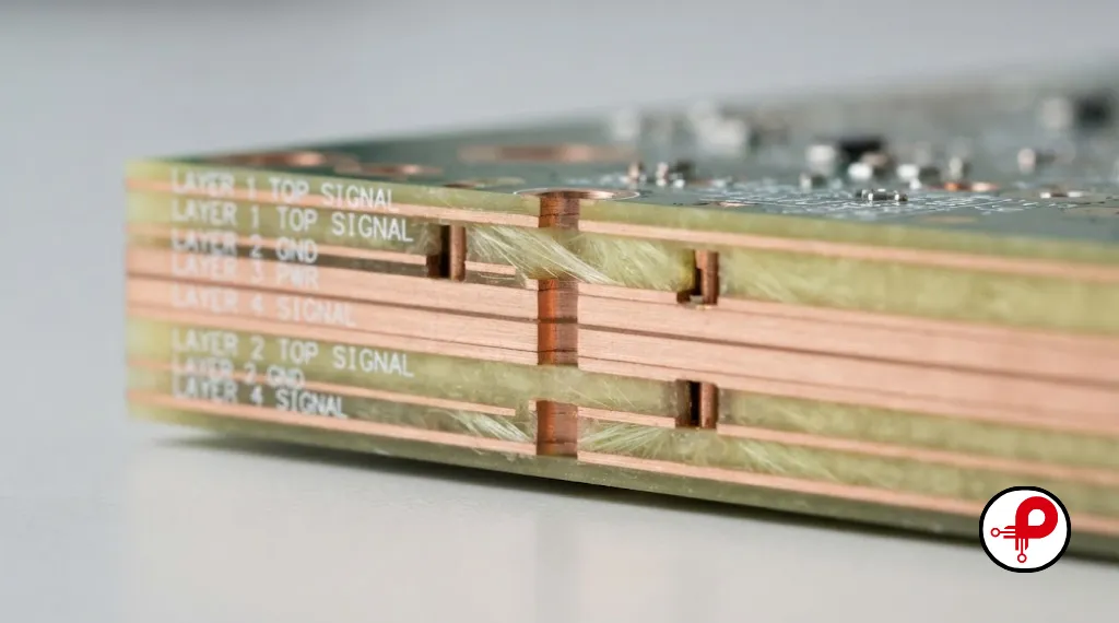
High-speed PCB design rules exist because at gigahertz frequencies, even small layout errors create reflections, timing mismatches, and radiated EMI that a slower board would never show. The core principle is that high-speed signals propagate as electromagnetic fields between the trace and its reference plane, so controlling that environment is the whole game.
Key high-speed PCB design rules to apply:
Maintain targets like 50 ohms (single-ended) or 90/100 ohms (differential) by balancing trace width, copper thickness, and dielectric height with your fabricator’s stack-up calculator.
Route next to a solid reference plane. Never route two high-speed layers directly adjacent (broadside coupling), as this increases crosstalk and creates impedance discontinuities.
Avoid 90-degree bends. Sharp corners change trace width at the vertex and cause impedance discontinuities; use 45-degree or rounded corners instead.
Keep differential pairs matched in length, spacing, and impedance (typically within a few mils) to preserve signal quality on interfaces like USB, HDMI, and PCIe.
Never route across a reference plane split. This forces return current to detour, adding noise and jitter; if unavoidable, add stitching capacitors near the transition.
Minimize vias on critical nets to reduce parasitic inductance. When a layer change is required, place ground vias near the signal via to preserve the return path.
If your product includes a wireless module, these same high-speed PCB design rules apply directly to antenna matching and RF traces. Our practical ESP32 PCB design guide shows how these rules play out on a real Wi-Fi and Bluetooth layout, and our explainer on how Bluetooth works in embedded systems is useful background if you are new to RF layout.
7. Design Rules for Analog, Digital, and Mixed-Signal Circuits
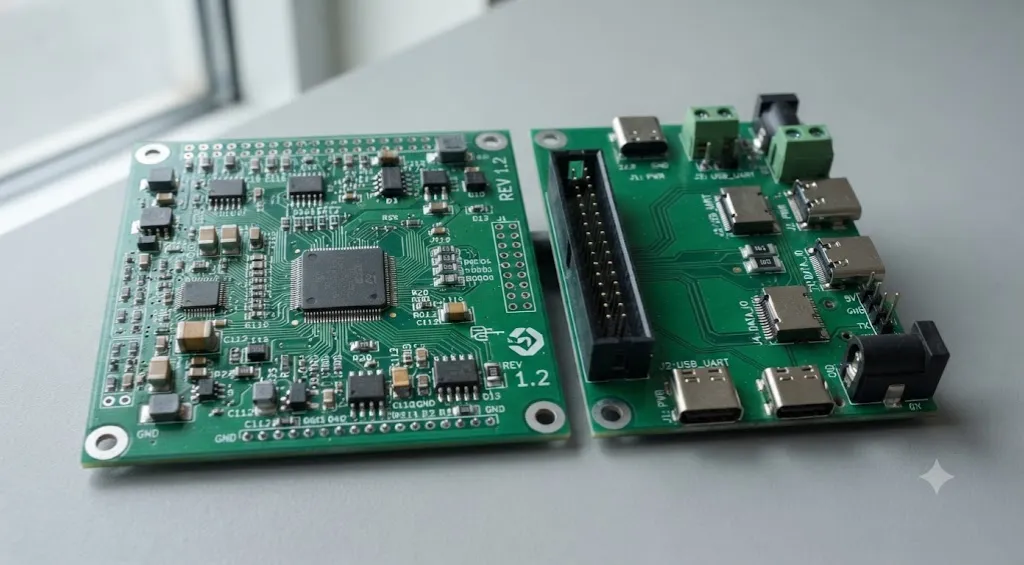
PCB design rules for analog circuits, PCB design rules for digital circuits, and PCB design rules for mixed signal circuits are not interchangeable, and treating them the same is a common source of noise problems.
Analog circuits are sensitive to small voltage variations, so PCB design rules for analog circuits emphasize short, direct traces for low-level signals, dedicated ground returns for sensitive nets, and physical separation from any switching or digital circuitry. Star grounding is often preferred over a shared plane for precision analog sections.
Digital circuits tolerate more noise but generate it in large quantities, especially at fast switching edges. PCB design rules for digital circuits focus on controlled impedance for clock and bus lines, solid uninterrupted ground planes, and adequate decoupling at every IC.
Mixed-signal boards need both approaches applied at once, without letting them interfere with each other. PCB design rules for mixed signal circuits typically call for a single-point ground connection between analog and digital ground regions, physical separation on the board (analog components grouped away from digital switching components), and careful routing so no digital trace ever crosses an analog ground boundary. Analog-to-digital converters usually sit right at this boundary and deserve the most placement discipline of any component on the board.
8. Design Rules for High Voltage and High Frequency Circuits
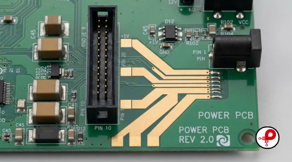
PCB design rules high voltage designs demand the largest safety margins on this list, because the consequence of a mistake is arcing, insulation breakdown, or fire risk rather than a noisy signal. For every 100V increase, plan on roughly 10 mils of additional external-layer clearance as a starting point, then verify against the full IPC-2221 spacing table for your exact voltage and altitude. Creepage distance, not just clearance, becomes the limiting factor in humid or contaminated environments, since surface conduction can bridge a gap that would otherwise be safe through air.
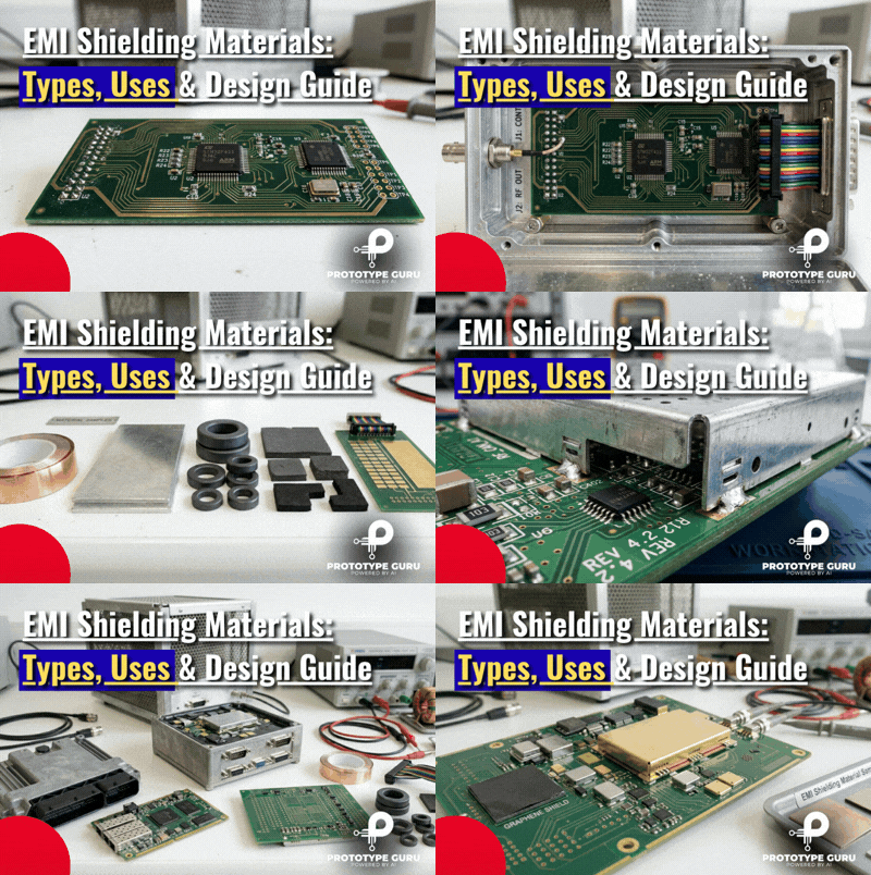
PCB design rules for high frequency work, on the other hand, are less about raw spacing and more about dielectric behavior. Standard FR-4 works for many designs, but above roughly 10 GHz its dielectric loss becomes significant enough to distort the signal, which is why RF and mmWave boards often shift to low-loss laminates. High-frequency layouts also benefit from grouping noisy components like ADCs and switching regulators toward the center of the board rather than the edges, which reduces radiated emissions. For a deeper look at diagnosing these issues after the fact, see our guide to EMI issues, causes, examples, and fixes and our walkthrough of EMI shielding materials and types.
9. Grounding, Stack-Up, and EMI Control
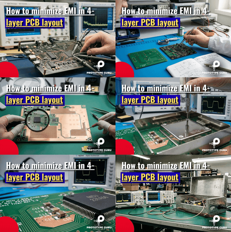
Almost every EMI problem I have diagnosed over the years traces back to one of three areas: component placement, grounding, or stack-up, rather than some mysterious external source. Getting the stack-up right early prevents most of it.
A well-planned stack-up keeps every signal layer adjacent to an uninterrupted ground or power plane, which provides a low-inductance return path and shields the signal from neighboring layers. For a 4-layer board, a common and effective arrangement is Signal, Ground, Power, Signal, since it gives every signal layer a solid reference. Our guide on minimizing EMI in a 4-layer PCB layout walks through this exact configuration in more detail. For 6 and 8-layer boards, the general principle scales: keep signal layers paired with adjacent reference planes, place power planes toward the center where their capacitance best supports decoupling, and mirror the stack-up for mechanical symmetry so the board does not warp during reflow.
Grounding rules worth building into every layout:
Use solid, unbroken ground planes wherever possible, and never route a high-speed trace across a plane split.
Keep return current loop areas small by routing signal and return paths close together to reduce electromagnetic interference.
Add stitching vias around board edges and near connectors to tie ground layers together and contain EMI.
Separate analog and digital ground regions with a single-point connection rather than allowing them to merge freely.
If your product needs to pass regulatory testing, it is worth reviewing these choices against electromagnetic compatibility testing requirements before committing to a final stack-up, since a redesign after a failed test is far more expensive than one caught during layout review.
10. Setting Design Rules in Altium, KiCad, and JLCPCB
Every major ECAD tool lets you encode circuit board design rules directly into its Design Rule Checker, but the workflow differs slightly by platform.
| Platform | How Design Rules Are Set | Best For |
|---|---|---|
| Altium | Unified constraint manager with live DRC as you route; defaults to 10 mil track and spacing rules out of the box | Professional and enterprise-grade multilayer boards |
| KiCad | Design Rules Editor under board setup; free and open source with strong community libraries | Startups, hobbyists, and teams on a budget |
| JLC PCB | Built directly into EasyEDA’s menu, or manually entered into Altium/KiCad DRC using JLCPCB’s published capabilities page | Fast-turn prototyping and low-cost small-batch production |
Regardless of platform, the same principle applies: define your required PCB design rules clearance, minimum trace and space, and drill sizes based on your actual fabricator’s capabilities, not generic defaults, then let the DRC catch violations live as you route rather than after the fact. If you are unsure which tool fits your project, our overview of the Complete Electronic Product Design Workflow and our guide to hardware development for startups both cover how to choose a toolchain that matches your team’s stage and budget.
11. Step-by-Step Workflow for Applying Circuit Board Design Rules
1. Schematic Organization
Start with a clean schematic. Group circuits by function using hierarchical sheets, such as power supply, MCU core, and RF section, since a messy schematic gets amplified into a messy layout.
2. Stack-up Definition
Define your stack-up before placement. Decide layer count, reference plane adjacency, and target impedance early, ideally in consultation with your fabricator’s stack-up calculator.
3. DRC Rules Entry
Enter your design rules into the DRC. Pull minimum trace and space, drill size, and annular ring values from your fabricator’s capabilities page, not from memory.
4. Functional Placement
Place components by function. Keep power circuits, sensitive analog sections, and high-speed digital blocks physically grouped and separated from each other.
5. Power and Ground Routing
Route power and ground first. Route the highest current paths before board space is consumed by lower-priority nets.
6. High-Speed Signal Routing
Route high-speed and differential nets next. Apply length matching, controlled impedance, and reference plane rules while board space is still open.
7. Ground Pour and Stitching
Fill remaining space with ground copper. Stitch ground pours together with vias to reduce loop area and improve EMI performance.
8. Final DRC Verification
Run a full DRC pass. Resolve every clearance, width, and annular ring violation before moving to review.
9. Design Review
Perform a design review. Have a second engineer or your fabricator’s layout service check the board against DFM rules before releasing Gerbers.
10. Manufacturing Submission
Generate manufacturing files and submit. Include Gerbers, drill files, a pick-and-place file, and a bill of materials, then confirm receipt with your chosen partner.
12. Common PCB Design Mistakes to Avoid
| Mistake | Consequence | Fix |
|---|---|---|
| Ignoring fabricator DFM limits | Manufacturing hold or rejection | Pull actual capability values before starting layout |
| Routing high-speed traces over plane splits | EMI, jitter, signal reflections | Reroute or add stitching capacitors at the transition |
| Undersized trace width for current | Overheating, reliability failure | Use IPC-2152 or a trace width calculator |
| Mixing analog and digital grounds freely | Noise coupling, measurement errors | Use single-point ground connection |
| Skipping silkscreen clearance | Illegible labels, assembly errors | Follow IPC font height and stroke width minimums |
| No decoupling near IC power pins | Voltage droop, glitches | Place capacitors as close to the pin as physically possible |
Our dedicated article on PCB design mistakes expands on each of these with real examples from past projects, and it pairs well with our notes on reverse engineering electronic circuits if you are trying to learn from an existing board before laying out your own.
13. Real World Example

A recent consumer electronics client came to us with a battery-powered device that intermittently reset under load. The schematic was correct, but the layout routed the switching regulator’s high-current loop across a gap in the ground plane, and the decoupling capacitor sat nearly half an inch from the microcontroller’s power pin. Applying basic circuit board design rules, tightening the current loop, closing the ground plane gap, and moving the capacitor within 2 mm of the pin, resolved the resets without a single component change. This is a textbook example of why layout discipline matters as much as component selection, a theme we explore further in our consumer electronics product design guide. If the product also involves a rechargeable cell, our lithium-ion battery protection circuit guide covers layout considerations specific to that circuitry.
14. Expert Tips
Pro Tip: Build your DRC rule set from your fabricator’s published capabilities before you place a single component, not after routing is complete. Retrofitting design rules onto a finished layout almost always forces a partial reroute.
Pro Tip: When in doubt on clearance for a new voltage level, calculate it against IPC-2221, then add margin for your worst-case environment (humidity, altitude, contamination) rather than designing to the bare minimum.
Warning: Do not trust default DRC settings in any ECAD tool. Altium’s out-of-the-box 10 mil defaults, for example, will not automatically match your fabricator’s actual capability or your product’s voltage and frequency requirements.
Pro Tip: Order a small pilot run before committing to full production volume. Automated inspection at this stage catches problems a visual check misses. Our explainer on automated optical inspection shows how fabricators catch these issues before they reach you.
15. PCB Design Rules Checklist Before Manufacturing

Final PCB Design Verification Checklist
- Stack-up finalized and matched to fabricator capabilities
- Minimum trace and space set per fabricator DFM rules
- Clearance values verified against IPC-2221 for actual operating voltage
- Trace widths checked against current-carrying requirements (IPC-2152)
- High-speed nets routed adjacent to solid reference planes
- No traces routed across plane splits
- Differential pairs length-matched and impedance-controlled
- Analog and digital grounds separated with single-point connection
- Decoupling capacitors placed within 2 mm of IC power pins
- Silkscreen text meets minimum font height and stroke width
- Drill-to-drill and drill-to-copper spacing verified
- Full DRC run with zero unresolved violations
- Gerbers, drill files, BOM, and pick-and-place file generated and checked
- Design reviewed by a second engineer or fabricator’s DFM service
16. Tools and Resources
For calculating and verifying circuit board design rules, the following tools are worth keeping bookmarked:
- IPC-2221 and related standards for the authoritative source on clearance and creepage requirements, available through IPC’s official standards library.
- Altium Designer’s constraint manager, documented in Altium’s own PCB trace and pad clearance guide, for live DRC while routing.
- KiCad, a free, open-source alternative with a strong Design Rules Editor, available at kicad.org.
- JLCPCB’s capabilities page, useful for confirming current minimum trace, space, and drill values before finalizing a design rule set.
- Trace width and impedance calculators, commonly built into ECAD tools or available as standalone field solvers for controlled-impedance work.
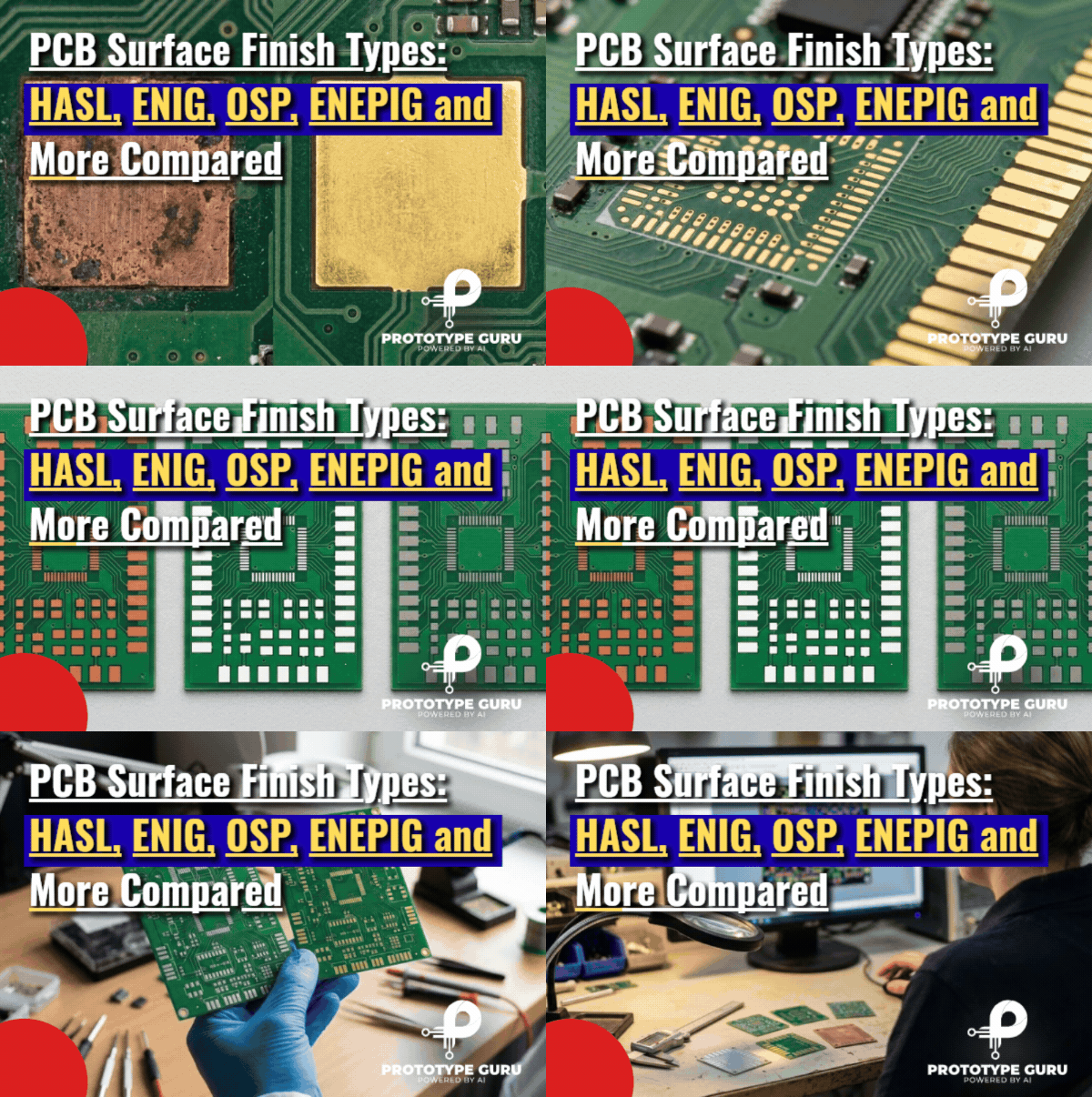
Once your design rules are locked in and your layout passes DRC, the next step is preparing for fabrication. Our overview of the PCB manufacturing process and surface mount technology soldering guide cover what happens after your Gerbers leave your desk. If you are building around a specific platform, our Arduino Uno Q guide and ESP32 audio player project show these design rules applied on real boards. For teams scaling toward mass production, our notes on industrial product design engineering and current PCB design trends are worth a read, and if you are manufacturing in the United States specifically, see our guide to electronics prototyping and product design in the USA.
17. Frequently Asked Questions
What are the basic PCB design rules every beginner should know?
↑What is the minimum clearance for PCB design rules?
↓How do I set PCB design rules in Altium or KiCad?
↓What is the difference between PCB design rules and PCB design standards?
↓Do JLC PCB design rules differ from standard IPC values?
↓What PCB design rules apply to high-speed signals?
↓Why do PCB design rules differ for analog and digital circuits?
↓Where can I find a PCB design rules PDF for reference?
↓18. Conclusion
Circuit board design rules are not a bureaucratic checkbox exercise. They are the accumulated lessons of an industry that has spent decades learning, sometimes the hard way, exactly how close two conductors can sit, how wide a trace needs to be, and how a ground plane needs to be structured before a board becomes unreliable or unmanufacturable. Whether you are working through basic PCB design rules on your first project or fine-tuning high-speed PCB design rules for a gigabit interface, the underlying discipline is the same: define your constraints early, enter them into your DRC, and verify them against your actual fabricator’s capabilities rather than generic defaults.
Treat the checklist in this guide as a living document you return to before every tape-out. It is far cheaper to catch a clearance violation on your screen than to discover it after a thousand boards have already been fabricated. If you would rather have an experienced team apply these circuit board design rules for you, from schematic capture through DFM-checked Gerbers, reach out and we will walk your project through the same process outlined above.