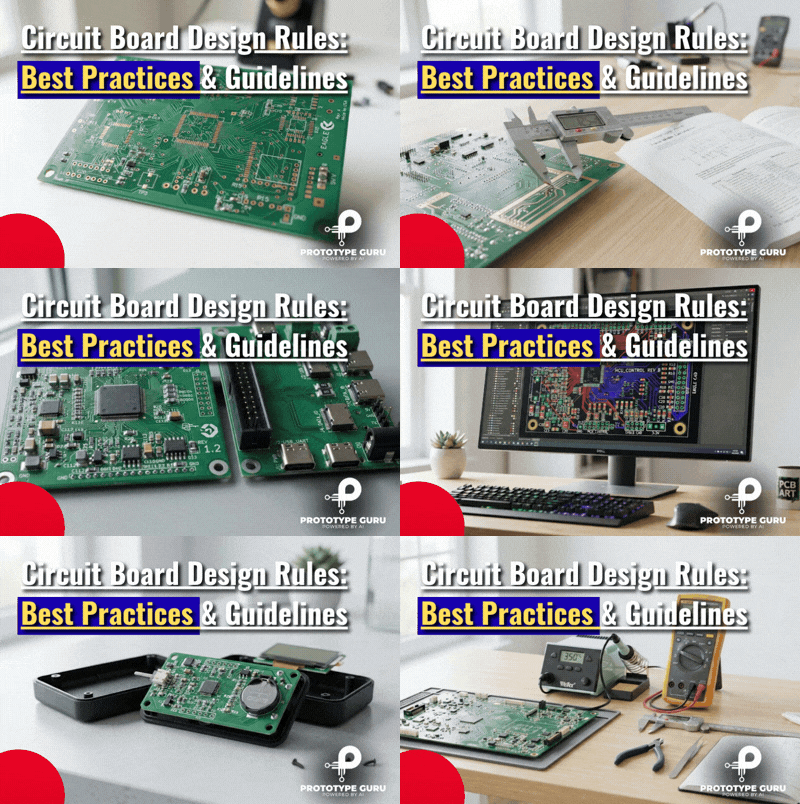









PCB layout best practices are the difference between a board that works the first time it powers on and one that comes back from the lab with a list of mystery failures. I have spent more than eight years routing boards for startups and established manufacturers alike, and almost every field failure I have debugged traces back to a handful of layout decisions made early in the design, not late in the fabrication process. This guide walks through the same PCB layout best practices I use on real projects, from component placement through thermal management, so you can catch problems on the screen instead of on the bench.
If you are building your first prototype or you are a hardware startup preparing for your first production run, this article is written for you. We will cover placement, stack up, grounding, impedance, EMI, vias, thermal design, and manufacturability, and we will back every recommendation with the same IPC standards and engineering reasoning that professional PCB design services use every day
What Is PCB Layout and Why It Decides Product Reliability
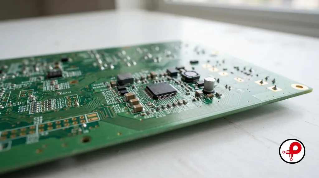
PCB layout is the process of translating a schematic into a physical printed circuit board, deciding where every component sits, how every trace routes, and how every layer of copper is arranged. A schematic tells you what should be connected. Layout tells you how well those connections actually behave once real current and real signals move through them.
This matters because a printed circuit board is never just a set of wires. At any frequency above a few megahertz, a trace behaves like a transmission line, and its physical geometry, not just its electrical connection, determines whether a signal arrives clean or arrives distorted. Good PCB layout design controls impedance, manages return current, keeps noisy circuits away from sensitive ones, and gives every component the thermal and mechanical support it needs to survive years in the field.
Startups often treat layout as a checkbox step after the schematic is done. Experienced hardware teams treat it as its own engineering discipline, because a board that looks correct in the schematic can still fail electromagnetic compatibility testing, overheat in enclosure, or simply refuse to boot reliably if the physical layout ignores these PCB design best practices. If your product will go through PCB manufacturing and assembly at any real volume, the layout stage is where you either bank reliability or borrow trouble from your future self.
Quick Reference Checklist for PCB Layout Best Practices
Before we go deep into each topic, here is the condensed version I hand to junior engineers on my team.
| Layout Area | What to Check | Why It Matters |
|---|---|---|
| Component placement | Group by function, keep high speed parts close together | Shorter traces mean fewer signal integrity problems |
| Stack up | Every signal layer next to a solid reference plane | Controls impedance and return path |
| Grounding | No split planes under high speed traces | Prevents EMI and ringing |
| Trace width | Sized to IPC-2221 or IPC-2152 current tables | Avoids overheating and voltage drop |
| Differential pairs | Matched length, constant spacing | Preserves common mode noise rejection |
| Decoupling | Capacitors placed at the pin, smallest value closest | Cleans local power supply noise |
| Vias | Minimized on high speed nets, backdrilled above 3 Gbps | Removes resonant stubs |
| Thermal | Thermal vias under hot components, adequate copper | Extends product lifespan |
| DFM/DFA | Panelization, silkscreen, courtyard spacing checked | Reduces assembly defects and cost |
Keep this table nearby. Every section below expands on one row.
Component Placement Best Practices
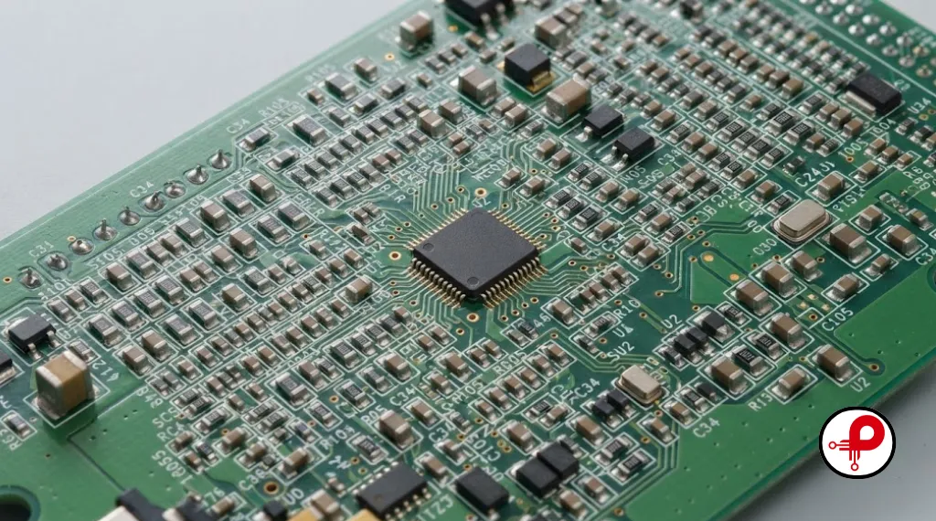
PCB component placement is the first decision that shapes everything downstream, and it is also the easiest one to get wrong under deadline pressure. I always start placement in three passes rather than one.
Pass one, functional zoning. Group parts by what they do: power input and regulation, the digital core, analog or RF sections, and connectors. Keep noisy switching regulators away from sensitive analog front ends. If you are designing a wireless product, this is the same zoning logic covered in our guide on how to make a Bluetooth device, where RF sections need physical separation from digital switching noise.
Pass two, critical path placement. Place your highest speed components, crystals, memory, and RF modules first, and route their critical nets before anything else competes for board space. Crystals should sit as close as possible to their IC with short, guarded traces, since crystal traces are notoriously sensitive to coupling.
Pass three, connectors and mechanical constraints. Fit connectors, mounting holes, and mechanical keep outs last, after your electrical zones are locked. This order feels backward to newcomers who want to place the enclosure connectors first, but doing it this way protects your signal integrity and only adjusts board outline and connector position afterward.
A few additional PCB layout tips for placement that consistently pay off:
Keep decoupling capacitors within a few millimeters of the IC power pin to ensure low-inductance paths, rather than placing them “somewhere nearby.”
Orient polarized components consistently across the board. This reduces assembly errors and simplifies visual inspection during the manufacturing process.
Leave adequate clearance around tall components. In wave soldering, tall parts can shadow the solder wave, preventing proper solder fillet formation on smaller parts behind them.
Match component footprints exactly to the manufacturer datasheet. Avoid modifying or creating library parts from memory to prevent fitment issues during assembly.
Good placement is also where you prevent many of the issues discussed in our roundup of PCB design mistakes, most of which start as placement shortcuts rather than routing errors.
PCB Stack Up Design for Signal Integrity
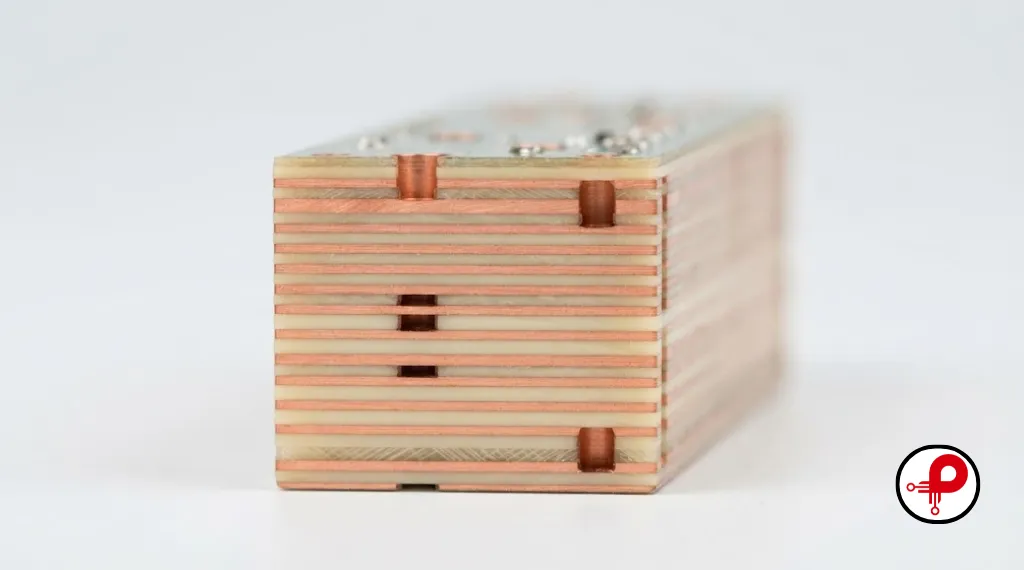
Your stack up is the foundation that every other layout decision builds on. A poorly planned stack up cannot be fixed by clever routing later, no matter how careful the designer is.
The core rule of PCB stack up design is simple: every high speed signal layer should have a continuous, unbroken reference plane, ground or power, directly adjacent to it. This keeps the loop inductance low and gives return current a short, predictable path.
For most product level boards, here is how layer count typically maps to capability:
2 Layers
Fine for simple, low-speed designs. Since there is no internal reference plane, signal integrity is limited due to the lack of a controlled return path.
4 Layers
The realistic minimum for most consumer and IoT products. A signal, ground, power, and signal arrangement is a common and highly effective configuration.
6 Layers
Adds internal stripline routing for sensitive signals. This is essential once you introduce high-speed interfaces like USB 3.0, high-speed memory, or RF circuitry.
8 or More Layers
Required for dense, high-performance layouts with multiple shielded routing channels, typically found in professional industrial and networking equipment.
When you are deciding between these options for a new product, it helps to weigh custom PCB design vs off the shelf solutions, since a custom stack up gives you control that a generic reference design usually cannot.
A properly documented stack up also states the dielectric constant, copper weight per layer, and target impedance for each signal class, so your fabricator can build coupons and verify the finished board actually matches what you simulated. Cadence’s engineering resources on <cite index=”6-1″>the connection between signal integrity and power integrity in PCB design describe how layout decisions around trace geometry, stackup configuration, and material choices directly impact signal clarity and power stability</cite>, which is exactly why stack up planning happens before routing, not after.
Ground Plane Design and Return Current Paths
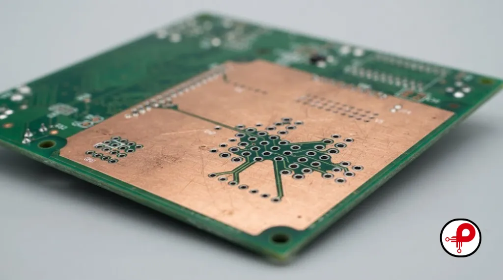
If there is one PCB layout best practice that separates reliable boards from unreliable ones, it is respecting the return current path. Every signal current that leaves a driver has to return to its source, and that return current always takes the path of least inductance, which in a well designed board is the plane directly underneath the trace.
The mistake I see most often, even from experienced engineers, is routing a high speed trace across a split or a gap in the reference plane. As one high speed design guide puts it plainly, <cite index=”3-1″>crossing a gap in the reference plane forces return current to take a long, inductive loop around the split, which acts like a slot antenna that radiates EMI and damages signal integrity</cite>. That single mistake can turn a clean signal into a source of radiated emissions failures during compliance testing.
Practical PCB ground plane design rules I follow on every board:
- Use a solid, unbroken ground plane under any trace running faster than a few megahertz.
- If a signal must cross a plane split for unavoidable reasons, add a stitching capacitor near the crossing to give return current a short path between reference planes.
- Stitch ground planes together with vias every quarter wavelength or less at your highest signal frequency of concern.
- Avoid routing digital return currents through the same plane area as sensitive analog return currents.
Getting grounding wrong is one of the fastest ways to trigger EMI issues, causes, examples, and fixes late in a project, usually right before a compliance test deadline. It is far cheaper to fix at the layout stage than after silkscreen and mechanical tooling are locked.
PCB Trace Width and Controlled Impedance
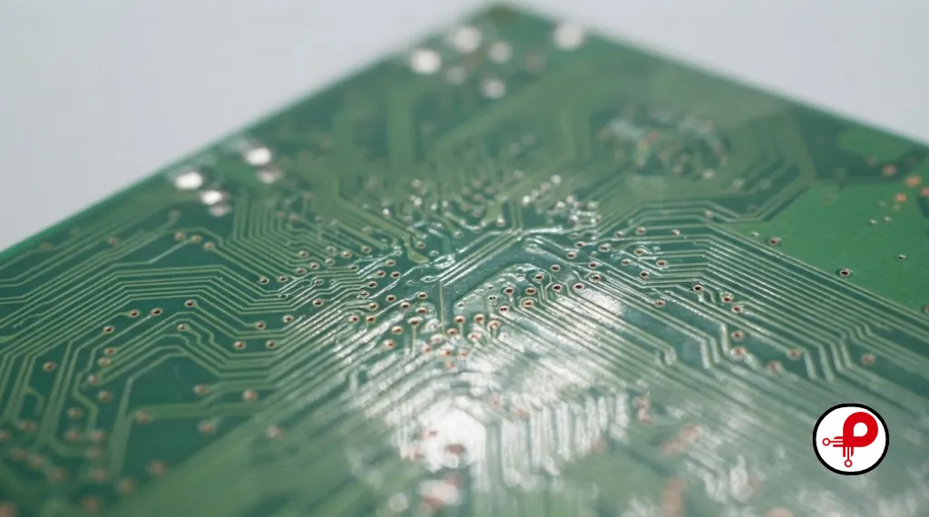
PCB trace width is not a cosmetic choice. It determines how much current a trace can carry without overheating and, for high speed signals, whether the trace presents the impedance your driver and receiver expect.
For current carrying capacity, the industry reference is IPC-2221, which uses the classic formula I = k × ΔT^0.44 × A^0.725, where k is 0.048 for external layers and 0.024 for internal layers. In practice, <cite index=”14-1″>internal layers require roughly two to three times wider traces than external layers for the same current, because internal layers have no direct air cooling and rely entirely on conduction through the board substrate</cite>. If you are sizing power traces, that difference alone should change your layer assignment for anything carrying meaningful current.
For more accurate results on dense, high current boards, many engineers now cross check against IPC-2152, since <cite index=”19-1″>IPC-2152 generally allows slightly narrower trace widths than IPC-2221 for the same current, because it accounts for modern practices such as copper pours and planes that help spread heat</cite>.
Practical trace width guidelines:
Use a 10 mil minimum width for typical signal traces on a 1oz copper board. This is primarily to ensure manufacturing reliability and prevent etching defects.
Avoid guessing when sizing power traces. Use an IPC-2221 or IPC-2152 calculator to determine appropriate widths, especially for currents exceeding 1A.
For impedance-critical nets, calculate width and spacing based on your specific stack-up dielectric thickness and copper weight rather than relying on generic rules of thumb.
Always verify your fabricator’s tolerances for copper thickness and dielectric constant (Dk) before finalizing widths for impedance-sensitive nets.
This is one area where I always recommend working with your fabrication partner early. The stack up calculator your fabricator uses reflects their real process tolerances, and no simulation replaces that verification step once you move from prototype to full PCB manufacturing process runs.
Differential Pair Routing
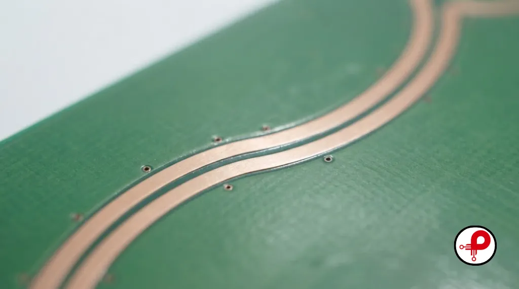
Differential pair routing shows up constantly in modern designs, from USB and HDMI to LVDS sensor links and high speed SerDes. The entire point of a differential pair is common mode noise rejection, and that only works if both traces see essentially the same environment along their length.
The two rules that matter most: <cite index=”2-1″>the two traces of a differential pair must be of equal length within a few mils, and they need constant spacing along their run</cite>. A common misconception is that tighter coupling between the two traces is always better. In reality, <cite index=”2-1″>maintaining a constant distance to the reference plane matters more for impedance stability than the distance between the two traces themselves</cite>.
Practical differential pair routing checklist:
- Route pairs together on the same layer whenever possible, and avoid splitting a pair across layers unless a via transition is unavoidable.
- Match length using small serpentine sections placed close to the source of the mismatch, not bunched at one end of the route.
- Avoid routing differential pairs over plane splits, for the same return path reasons that apply to single ended signals.
- Keep unrelated signals at least a few trace widths away from the pair to limit crosstalk pickup.
If your product includes wireless connectivity, differential routing discipline becomes even more important around the antenna feed and RF front end. Our guide on how Bluetooth works in embedded systems and IoT covers how layout choices in that section of the board directly affect range and reliability.
Power Distribution and Decoupling Capacitors
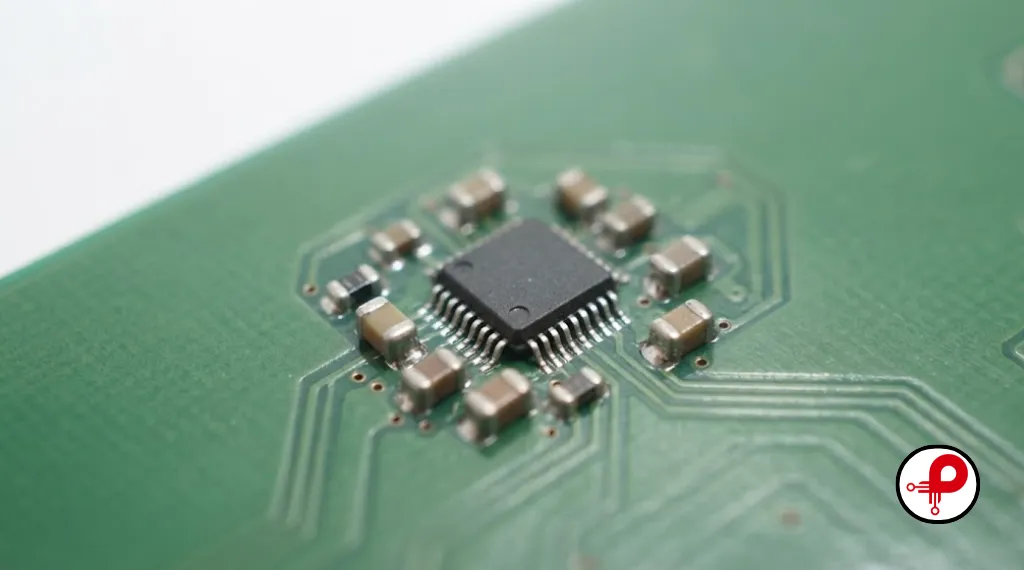
Power distribution PCB design is easy to underestimate because failures show up as vague symptoms, occasional resets, jitter, or intermittent glitches, rather than an obvious short. Modern ICs, FPGAs, and processors draw large current transients in nanoseconds, and if the power distribution network cannot supply that current cleanly, the supply voltage droops or rings right when the chip needs it most.
Decoupling capacitor placement is the fastest win here. Place the smallest value capacitor as close as physically possible to the IC power pin, since smaller capacitors handle higher frequency noise and physical distance adds inductance that defeats the capacitor’s purpose at high frequencies. Use a range of values, for example a small ceramic close to the pin and a larger bulk capacitor slightly further out, so you cover a wider noise frequency range.
Other power distribution PCB best practices:
Keep power plane copper as continuous as possible, and avoid narrow necks that create localized voltage drop or increase impedance.
Route the highest current paths first, before board space gets consumed by lower priority nets, ensuring adequate trace width for heat dissipation.
Use dedicated power and ground layer pairs directly adjacent to each other to minimize plane inductance and improve decoupling efficiency.
For battery-powered designs, protection circuitry deserves its own placement discipline, similar to the layout considerations in our lithium-ion battery protection circuit guide.
EMI Reduction in PCB Layout
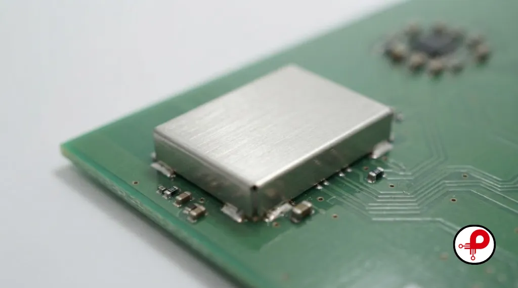
EMI reduction in PCB layout is where component placement, grounding, and stack up decisions all come together, because almost every EMI problem I have diagnosed traces back to one of those three areas rather than a mysterious external cause.
The most common and preventable EMI source is exactly what we covered in the grounding section: a high speed trace crossing a reference plane split, which turns the return current loop into an unintentional slot antenna. The second most common source is switching regulator layout, where a poorly placed switch node trace with a large loop area radiates broadband noise across a wide frequency range, an issue explored in depth in our piece on high frequency switching noise issues.
Practical EMI reduction techniques:
- Physically separate switching power supplies, fast digital clocks, and sensitive analog or RF sections into distinct board zones.
- Keep switch node copper area as small as practical while still meeting current requirements, since that node radiates the most.
- Add ground stitching vias around noisy sections to contain fields rather than letting them couple onto neighboring traces.
- Consider board level shielding for the most sensitive sections, and review our EMI shielding materials and types guide when layout alone cannot fully contain a noisy circuit.
- Budget time for electromagnetic compatibility testing early in your schedule, not as a last minute gate before launch.
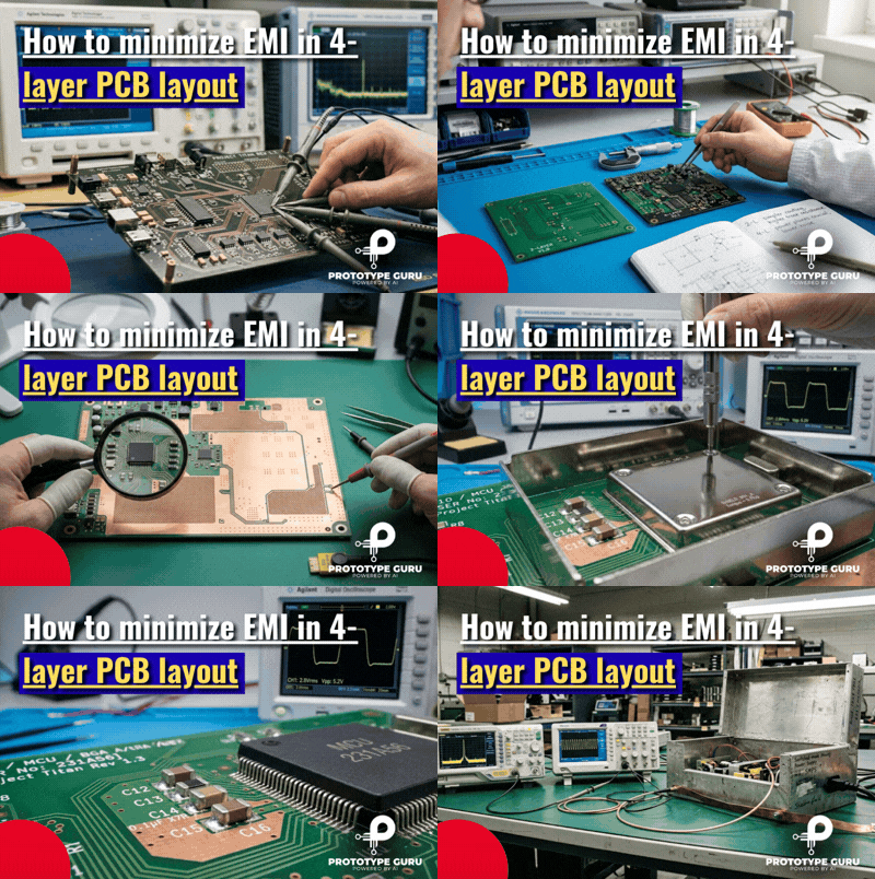
For a deeper technical breakdown of layer specific EMI control, our article on how to minimize EMI in a 4 layer PCB layout walks through layer assignment strategies specifically for the most common consumer product stack up. If your product includes switching power supplies, our guide on how EMI EMC filters reduce noise in power electronics is also worth reading before finalizing your power section layout.
Via Placement and Backdrilling
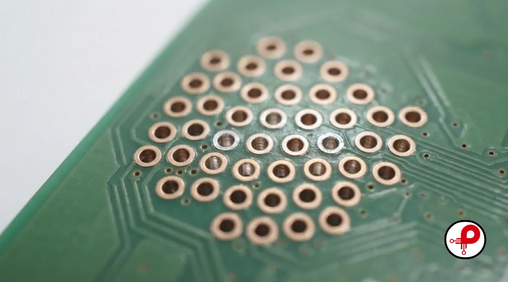
Vias are necessary for any multi-layer PCB layout, but every via you add to a high speed signal path introduces parasitic inductance and capacitance that acts like a small speed bump for the signal. On lower speed boards this barely matters. On high speed serial links it can be the difference between a clean eye diagram and a failed link.
Via stubs are the specific concern above a few gigabits per second. <cite index=”10-1″>Via stubs, the unused portions of through hole vias, act as resonant elements that cause signal reflections and insertion loss, and at data rates above roughly 3 Gbps these effects become significant.</cite> Backdrilling removes that unused stub by drilling out the barrel below the last layer the signal actually needs, and it is now a standard request for any board carrying PCIe, USB 3, or SerDes class signals.
Via placement best practices:
1. Minimize Via Count
Minimize via count on any net where the signal edge rate is fast enough to matter, and try to keep high-speed signals on a single layer when board space allows to reduce discontinuities.
2. Strategic Ground Vias
Place a ground via next to every signal via that changes layers, giving the return current a short, controlled path to follow the signal transition and maintain loop integrity.
3. Stub Elimination
Specify backdrilling with your fabricator for any via carrying signals above roughly 3 Gbps, or use via-in-pad structures with filled and capped vias where stub elimination is critical for performance.
4. BGA Via Considerations
Avoid placing vias directly under BGA components unless your fabricator confirms the process supports via-in-pad for that specific pitch to avoid assembly defects.
PCB Thermal Management
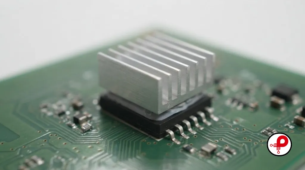
PCB thermal management gets far less attention than signal integrity, but it is just as often the reason a product fails in the field rather than in the lab, since thermal problems tend to show up only after months of real world operating cycles.
Every hot component, voltage regulators, power MOSFETs, RF power amplifiers, needs a defined thermal path off the board. Thermal vias placed under or near the component’s thermal pad conduct heat down to an internal copper plane or to a heatsink on the opposite side of the board. The more copper area you can dedicate to spreading that heat, the lower your steady state junction temperature will be.
Practical PCB thermal management guidelines:
- Use an array of thermal vias under any exposed pad package, rather than a single via, to reduce thermal resistance.
- Increase copper weight on layers carrying significant current or heat, since heavier copper conducts heat as well as current more effectively.
- Keep heat generating components away from heat sensitive components like crystals and precision analog references.
- Consider component orientation relative to expected airflow if the product includes a fan or vents.
Thermal design also intersects directly with your choice of enclosure and overall industrial product design engineering strategy, since the PCB cannot solve a thermal problem the enclosure was never designed to support.
Design for Manufacturability and Assembly
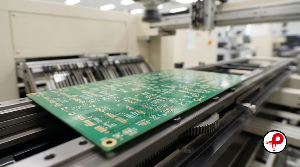
A layout can be electrically perfect and still cause expensive problems on the assembly line if it ignores design for manufacturability and design for assembly, commonly shortened to DFM and DFA.
Key DFM and DFA checks I run before releasing any board for fabrication:
- Confirm component courtyard spacing matches your assembler’s capability for hand soldering, selective soldering, or automated SMT reflow, since the tolerances differ meaningfully between these processes.
- Verify silkscreen text does not overlap pads or vias, and that reference designators remain legible after parts are placed.
- Check panelization strategy with your assembler before finalizing board outline and mounting hole locations.
- Confirm polarized component orientation is consistent and clearly marked to reduce placement errors during assembly.
- Review your design against your fabricator’s minimum trace, space, and via specifications rather than assuming default software rules are correct for your board.
These checks matter just as much for a five board prototype run as they do at volume, and they are exactly the kind of review covered in our guide to the PCB manufacturing and assembly process. If your board includes fine pitch components, our surface mount technology soldering guide covers the placement tolerances your layout needs to respect. Automated inspection is also worth planning for early, and our explanation of automated optical inspection working principle shows what a well laid out board makes easier to verify after assembly.
PCB Layout Best Practices by Application
Not every product needs the same layout rigor. Here is how I scope layout effort based on what the product actually needs to do.
| Product Type | Typical Layer Count | Priority Layout Focus | Common Pitfall |
|---|---|---|---|
| Consumer electronics | 2 to 4 layers | Cost, DFM, basic EMI control | Skipping ground plane on 2 layer boards |
| IoT and wireless devices | 4 layers | RF isolation, antenna keep out, EMI | Digital noise coupling into RF front end |
| Industrial equipment | 4 to 8 layers | Thermal management, robust power distribution | Underestimating trace width for high current paths |
| High speed digital / networking | 6 to 12+ layers | Controlled impedance, via stub elimination, stripline routing | Ignoring return path continuity across layer transitions |
| RF and wireless modules | 4 to 6 layers | Impedance matched RF traces, shielding, grounding | Treating RF traces like ordinary digital signals |
If your product falls into the consumer or IoT category, our consumer electronics product design guide walks through how layout decisions connect to overall product cost and schedule. For teams building around specific platforms, our ESP32 PCB design guide and our tutorial on an ESP32 audio player using the YX5300 MP3 module both apply these same principles in a real project context. Teams evaluating platform choices for a new wireless product may also find our Arduino Uno Q guide useful for early prototyping decisions before committing to a custom board.
Common PCB Design Mistakes That Undo Good Layout Work
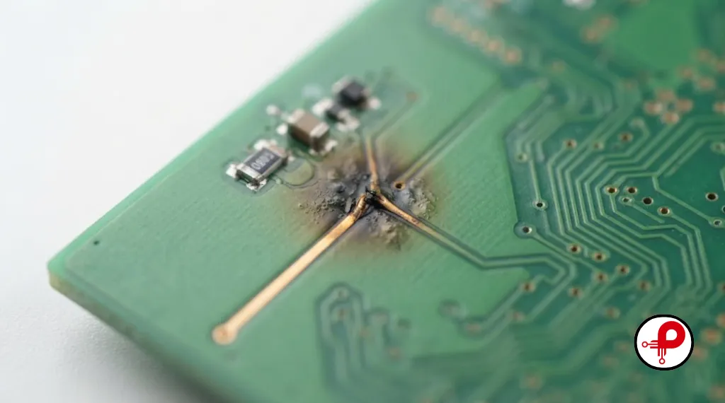
Even teams that know these PCB layout best practices in theory still make avoidable mistakes under deadline pressure. The most frequent ones I encounter, covered in more depth in our full breakdown of PCB design mistakes, include:
- Finalizing component placement before routing critical high speed nets, forcing awkward detours later.
- Splitting ground or power planes without considering which signals will cross that split.
- Copying trace widths from a previous project without recalculating current capacity for the new design’s requirements.
- Treating decoupling capacitor placement as a schematic detail rather than a layout critical decision.
- Skipping a DFM review because the board “looks simple,” which is exactly when small footprint or spacing errors slip through.
Awareness of current PCB design trends also helps teams avoid designing around outdated assumptions, particularly as component packages shrink and edge rates continue to increase across nearly every product category.
FAQ
What is the most important PCB layout best practice for beginners?
↑How do I choose the correct PCB trace width?
↓Is a 2-layer PCB enough, or should I use a 4-layer board?
↓What are the most common PCB layout mistakes?
↓How can I reduce EMI in a PCB layout?
↓When should I use differential pair routing?
↓Why is component placement important in PCB layout?
↓Why are PCB layout best practices important for product reliability?
↓Final Thoughts
PCB layout best practices are not a checklist you complete once and forget. They are a set of engineering habits, thinking about return current before you route a trace, sizing copper for real current rather than convenient defaults, and separating noisy circuits from sensitive ones before placement gets locked in. I have watched these habits save products from expensive respins more times than I can count, and I have watched their absence cause failures that looked mysterious until someone finally checked the ground plane.
If you are scoping a new hardware project and want a second set of experienced eyes on your layout before it goes to fabrication, that review is often the cheapest insurance you can buy for a product’s reliability. For startups building their first hardware product, our overview of hardware development for startups and our broader look at the complete electronic product design workflow both walk through where layout fits into the bigger picture from concept to production.
Sources referenced: Cadence PCB Solutions signal and power integrity resources, UltraLibrarian high speed PCB design guidelines, IWDF Solutions high speed PCB design guide, Schemalyzer PCB trace width guide, and DYC Electronic heavy copper trace width design reference.