













Staring at a finished layout and realizing there is nowhere for a test probe to land is a frustrating way to end a design cycle. It usually shows up late, right when a board is headed to a contract manufacturer, and it almost always means a redesign, a delayed schedule, or an expensive custom test fixture that was never part of the original budget.
PCB design for testability, often shortened to DFT, is the practice of building test access into a board from the very first layout decisions instead of bolting it on afterward. Done well, it barely changes how a board looks. Done poorly, or skipped entirely, it turns a routine production run into a troubleshooting exercise.
This guide walks through what design for testability actually means at the PCB level, the main testing methods it needs to support, concrete placement and spacing guidelines you can apply directly, and the mistakes that most often turn a testable board into an untestable one.
What Is PCB Design for Testability?
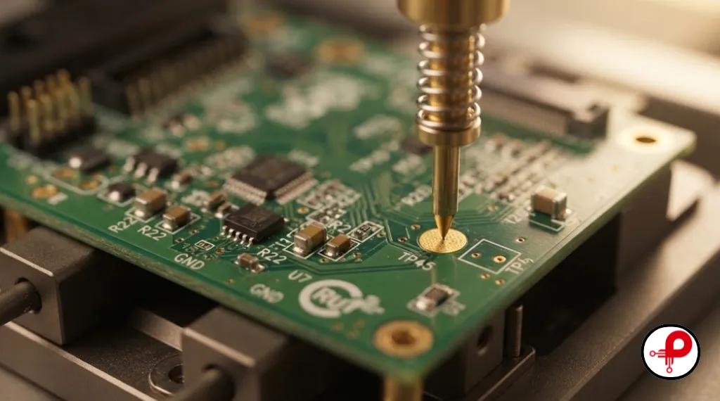
PCB design for testability is the set of layout and design decisions made during a board’s development that determine how easily it can be tested once it is manufactured and assembled. In practical terms, this means giving a test system, whether that is an in circuit tester, a flying probe machine, or a boundary scan chain, a reliable way to reach every net that actually matters for verifying the board works correctly. According to Altium, designing for testability is a critical step in the broader design for manufacturability process, and it centers on developing a consistent product at the lowest reasonable manufacturing cost while keeping defect rates acceptable. A board with excellent schematic design and flawless routing can still be a poor product if nobody thought about how it would be tested once it left the design software.
DFT is not a separate discipline bolted onto PCB design at the end. It is a mindset that runs alongside placement and routing from the earliest stages, the same way via design, thermal relief, or signal integrity planning does, and it deserves the same attention you would already give to something like your board’s solder mask design.
Why Design for Testability Matters in PCB Manufacturing

The case for DFT comes down to cost, speed, and confidence in what actually ships.
According to a detailed DFT resource from Anzer USA, proper design for testability practices catch between 85 and 95 percent of assembly defects before boards ever reach a customer. That is a meaningful difference compared to relying on functional testing alone, which only proves a board works under the specific conditions it was tested in, not that every individual connection was verified.
There is also a real financial argument. The same Anzer USA resource notes that proper DFT planning during layout can save between 5,000 and 15,000 dollars in redesigned fixtures and two to three weeks of production delay, figures that come directly from the cost of discovering testability problems after a board is already in fabrication rather than during layout review.
Skipping DFT does not remove the need for testing. It just moves the cost and the risk later in the process, usually to a point where fixing it is far more expensive.
Types of PCB Testing Methods You Need to Design For
Different test methods expect different things from your layout, so it helps to understand the main ones before setting placement rules.
In Circuit Testing (ICT)
Uses a bed of nails fixture, a plate of spring loaded pogo pins that make contact with dedicated test pads on the board. It checks a populated printed circuit board for manufacturing defects, but is only as good as the design of the board itself. If no test access has been provided by the designer, some tests simply will not be possible, no matter how capable the test system is.
Flying Probe Testing
Uses a small number of movable probes controlled by a program, rather than a fixed bed of pins. It needs no custom fixture, which makes it attractive for prototypes and low volume runs, though it is considerably slower per board than ICT.
Boundary Scan Testing (JTAG)
Standardized as IEEE 1149.1, boundary scan works by embedding test cells connected to each pin of a compliant device, which can drive or read signals across a board trace without requiring physical test probes at all. This makes it especially useful for dense boards using BGA or other packages where mechanical probe access is difficult or impossible.
AOI and AXI Inspection
Automated optical inspection (AOI) and automated x-ray inspection (AXI) round out the picture, checking solder joints and component placement visually or radiographically rather than electrically, which is particularly important for hidden connections under BGA packages.
Most production boards end up using a combination of these methods rather than relying on just one, and your DFT strategy should account for whichever combination your contract manufacturer plans to use.
ICT Test Point Placement Guidelines
Test point placement is where design for testability becomes concrete rather than conceptual.
AllPCB’s DFT handbook recommends placing a test point on every net where practical, since this gives the most comprehensive ICT coverage possible. In practice, full coverage on every single net is not always cost effective for large or complex boards, so most teams work with their test engineering team to agree on a realistic target, commonly in the range of 85 to 90 percent of nets, prioritizing power lines, such as the rails coming off a DC to DC converter or a power supply filtering stage, and high speed signals above roughly 100 MHz where defects would cause the most significant downstream problems.
A few placement principles come up consistently across manufacturer guidance:
Critical Signal Priority
Prioritize test points on nets connected to power rails, clocks, resets, and other control critical signals first, and give the same priority to nets feeding a low power circuit design where a missed connection is harder to catch functionally.
Component Clearance
Keep test points away from tall components, since probes need clear vertical access.
Mechanical Obstruction Avoidance
Avoid placing test points too close to connectors or mechanical features that could obstruct a fixture.
Hard-to-Reach Components (BGAs)
Add test points on nets connected to hard to reach components, such as BGAs, even when the component itself cannot be probed directly, since verifying a connected net can indirectly confirm the component’s connection is sound.
Communication Bus Routing
Route accessible test points onto communication lines too, whether that’s an I2C, SPI or UART bus or an RS485 circuit, since these interfaces are often the first thing a test program checks.
Working with your contract manufacturer’s own DFT guidelines early, rather than after layout is finished, tends to prevent most of these conflicts before they become expensive.
Test Pad Size and Spacing Requirements
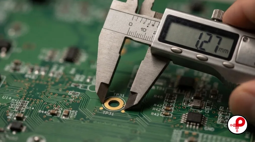
Physical dimensions matter more than most new designers expect, since a pad that is technically present but too small or too close to a neighbor can still fail during actual testing.
Guidance across manufacturer resources converges on a fairly consistent range. AllPCB recommends consistent pad sizes, typically between 0.8 and 1.2 millimeters in diameter, noting that smaller pads increase the risk of probe misalignment while larger pads waste board space you likely need elsewhere. Anzer USA gives a slightly more specific figure, recommending a minimum test point diameter of 40 mils, or 1.0 millimeter, with 50 mil, or 1.27 millimeter, center to center spacing for reliable pogo pin contact.
On clearance, AllPCB recommends maintaining at least 2.5 millimeters between individual test points to avoid probe interference, along with a minimum of 3 millimeters of clearance from tall components such as capacitors or connectors that could physically block probe access. This is also where your thermal relief pattern around a test pad matters, since a pad tied directly into a large copper pour without relief can make the pad harder to solder cleanly and, in some fixtures, affect probe contact reliability. For sensitive analog circuits, keeping test points at least 5 millimeters, or roughly 200 mils, away from high impedance nodes helps avoid the probe itself affecting signal integrity during the measurement, and the same clearance thinking applies around surge protection components, where a probe sitting too close to a protective device can distort the very measurement you’re trying to take.
| Parameter | Typical guideline |
|---|---|
| Test pad diameter | 0.8 to 1.2 mm, commonly cited as 1.0 mm minimum |
| Center to center spacing | 1.27 mm (50 mils) minimum |
| Clearance between test points | 2.5 mm minimum |
| Clearance from tall components | 3 mm minimum |
| Clearance from high impedance analog nodes | 5 mm (roughly 200 mils) |
| Practical test coverage target | 85 to 90 percent of nets |
These numbers are starting points, not absolute law. Your specific contract manufacturer’s fixture tooling, pogo pin selection, and board density will always take priority over a general guideline, which is exactly why requesting their DFT document before finalizing layout is worth the extra step.
Single Sided vs Double Sided Test Access

One of the more consequential early decisions in DFT is whether test points can live entirely on one side of the board.
Altium’s guidance on circuit board design for in circuit testers is direct about the cost implications here. Keeping test points to one side, typically the bottom or whichever side has the least circuit complexity, reduces the complexity of the test fixture significantly, which translates into a lower fixture cost and a better return on investment for the product overall. A double sided fixture requires probing hardware on both the top and bottom of the board simultaneously, which is mechanically more complex and considerably more expensive to build and maintain.
If top side access genuinely cannot be avoided, reserving it only for non critical nets, while keeping clocks, control pins, programming interfaces, serial data lines, and boundary scan connections on the bottom side, tends to be the more manageable compromise. This single decision, made early during placement, often has more impact on total test tooling cost than almost any individual test point rule.
Boundary Scan and JTAG Testing for Dense Boards
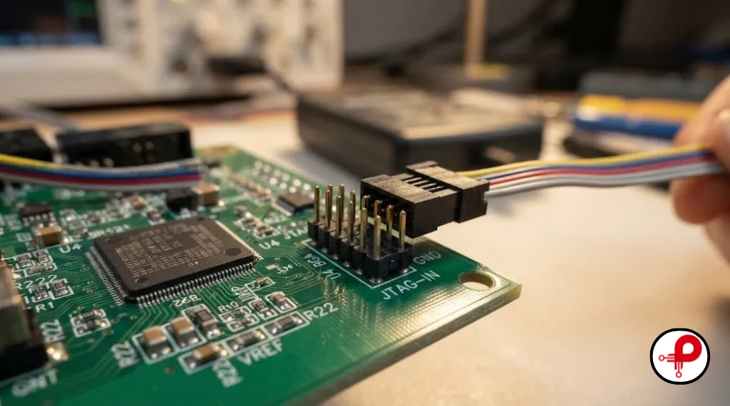
As package density has increased, boundary scan has moved from a nice to have feature to something close to a necessity for many modern boards.
The Joint Test Action Group developed the boundary scan specification that was standardized in 1990 as IEEE Std 1149.1, and it is now used so widely that the term boundary scan and the term JTAG are essentially treated as synonyms in most engineering conversations. Rather than relying on physical probes touching individual pads, boundary scan embeds test cells at each pin of a compliant device. Each cell can be programmed through the JTAG chain to drive a signal onto a pin, and the receiving cell at the other end of that trace can then be read back, confirming the connection is sound, all without a single mechanical probe touching the board.
This matters enormously for boards using BGA packages, chip scale packages, or any component where the physical pins are hidden underneath the package itself and simply cannot be reached by a bed of nails or a flying probe. If your design includes JTAG compliant devices, designing in a proper access header and following your device vendor’s boundary scan implementation guidance early in the schematic phase avoids having to retrofit test access after the fact, which is rarely a clean process. If you’re working with a specific part, our JTAG debugging guide for the ESP32-S3 walks through exactly this kind of access planning on a real, widely used chip.
Design for Testability and BGA or Hidden Pin Components
Ball grid array components deserve their own mention because they represent one of the most common testability headaches in modern PCB design.
By their physical construction, BGA packages hide their connections underneath the component body, which means neither ICT probes nor flying probes can make direct contact with the balls themselves once the part is soldered down. AllPCB’s DFT handbook for in circuit testing calls this out specifically, recommending that designers add test points on connected nets near a BGA even though the package itself cannot be probed, since this at least allows indirect verification that the component’s connections are electrically sound.
A few practical approaches help manage this constraint:
- Route critical BGA signals out to an accessible test point wherever board space allows
- Favor boundary scan compliant components when the design allows for it, since this sidesteps the physical access problem entirely for that device
- Where budget allows, plan for automated x ray inspection to visually confirm solder joint quality underneath the package, since this is currently the most reliable non electrical way to catch a poorly formed BGA joint
None of these fully replace direct probing, but combined, they typically close most of the visibility gap that BGA packages otherwise create.
Common DFT Mistakes That Undermine Testability
Even experienced designers repeat a handful of mistakes often enough that they are worth calling out directly.
1. Treating DFT as a Final Step
Treating DFT as a final step rather than a layout constraint. Adding test points after routing is complete usually means fighting for space that no longer exists, and it often results in compromised pad placement just to fit something in.
2. Ignoring CM Requirements
Ignoring the contract manufacturer’s specific fixture requirements. Generic DFT guidelines are a reasonable starting point, but every CM’s tooling has its own tolerances, pin diameters, and fixture constraints. Skipping this conversation until after fabrication tends to surface expensive surprises.
3. Clustering Test Points
Clustering test points in one area of the board. Concentrating test points together rather than distributing them evenly increases mechanical stress on the fixture in that zone and raises the risk of probe damage or bent pins over repeated test cycles.
4. Underestimating BGA Access
Underestimating BGA and fine pitch component access. As covered above, hidden pin packages need a deliberate plan, not an afterthought, particularly on boards with multiple BGAs.
5. Forgetting Mixed-Signal Sensitivity
Forgetting mixed signal and analog sensitivity. Placing a test point too close to a sensitive analog node without accounting for probe loading effects can introduce measurement error that looks like a board defect when it is actually a test artifact.
Most of these mistakes share a common root cause: DFT gets treated as something to solve after the design is functionally complete, rather than as a parallel requirement from the start.
DFT and Design for Manufacturability

Design for testability rarely stands alone in practice. It sits inside the broader discipline of design for manufacturability, or DFM, which covers everything from component selection and panelization to solder joint reliability and assembly yield.
Altium’s guidance frames DFT explicitly as a critical step within the DFM process, built around the goal of developing a consistent, manufacturable product at the lowest reasonable cost while keeping defect rates within an acceptable range. In practice, this means test point decisions should be reviewed alongside your DFM checklist, not as a completely separate exercise, since the two disciplines frequently influence the same layout decisions, such as component spacing, panel edge clearance, and overall board density.
Requesting both DFM and DFT guidelines from your contract manufacturer at the same time, rather than treating them as sequential steps, tends to produce a smoother handoff from design to production. IPC, the electronics industry standards body, publishes a full family of formal design and test documentation standards, including IPC-D-356 for bare board electrical test data and IPC-9252 for electrical test requirements, that many contract manufacturers reference directly in their own DFT documentation.
A Practical DFT Checklist for PCB Designers
Before releasing a board for fabrication, running through a short, concrete checklist tends to catch the majority of testability problems while they are still cheap to fix.
- Confirm test coverage on at least 85 to 90 percent of nets, prioritizing power, clock, and control critical signals
- Verify test pad diameter and spacing meet your contract manufacturer’s specific fixture requirements, not just a generic guideline
- Keep test points on a single side of the board wherever the design allows
- Provide a documented boundary scan access header for any JTAG compliant devices in the design
- Add indirect test points on nets connected to BGA or other hidden pin components
- Distribute test points evenly rather than clustering them in one region
- Maintain adequate clearance from tall components and sensitive analog nodes
- Request your contract manufacturer’s DFT and DFM documentation before finalizing layout, not after
Running this checklist during a design review, rather than only at final release, gives you room to adjust placement without disrupting a finished layout.
Frequently Asked Questions
1. What does DFT mean in PCB design?
↑2. How many test points does a PCB need?
↓3. What is the difference between ICT and flying probe testing?
↓4. Why is boundary scan important for BGA components?
↓5. Should test points be on one side of the board or both?
↓6. When should DFT be considered in the design process?
↓7. What are the standard size and spacing requirements for test points?
↓8. Do test points affect high-speed signal integrity?
↓Conclusion
PCB design for testability is not an optional finishing touch. It is a layout discipline that determines whether a board can actually be verified reliably once it leaves the design stage, and it has a direct, measurable effect on defect detection, fixture cost, and how smoothly a design moves from prototype to production. The specific numbers, test pad sizes, clearances, and coverage targets, matter less than the underlying habit of asking, at every placement decision, whether a probe or a boundary scan chain will actually be able to reach what needs to be reached.
Building that habit early, and confirming it against your specific contract manufacturer’s DFT and DFM guidelines before finalizing a layout, tends to save far more time and money than fixing testability problems after a board has already been fabricated.