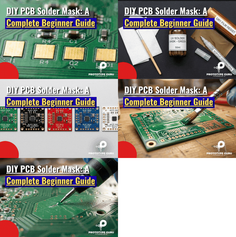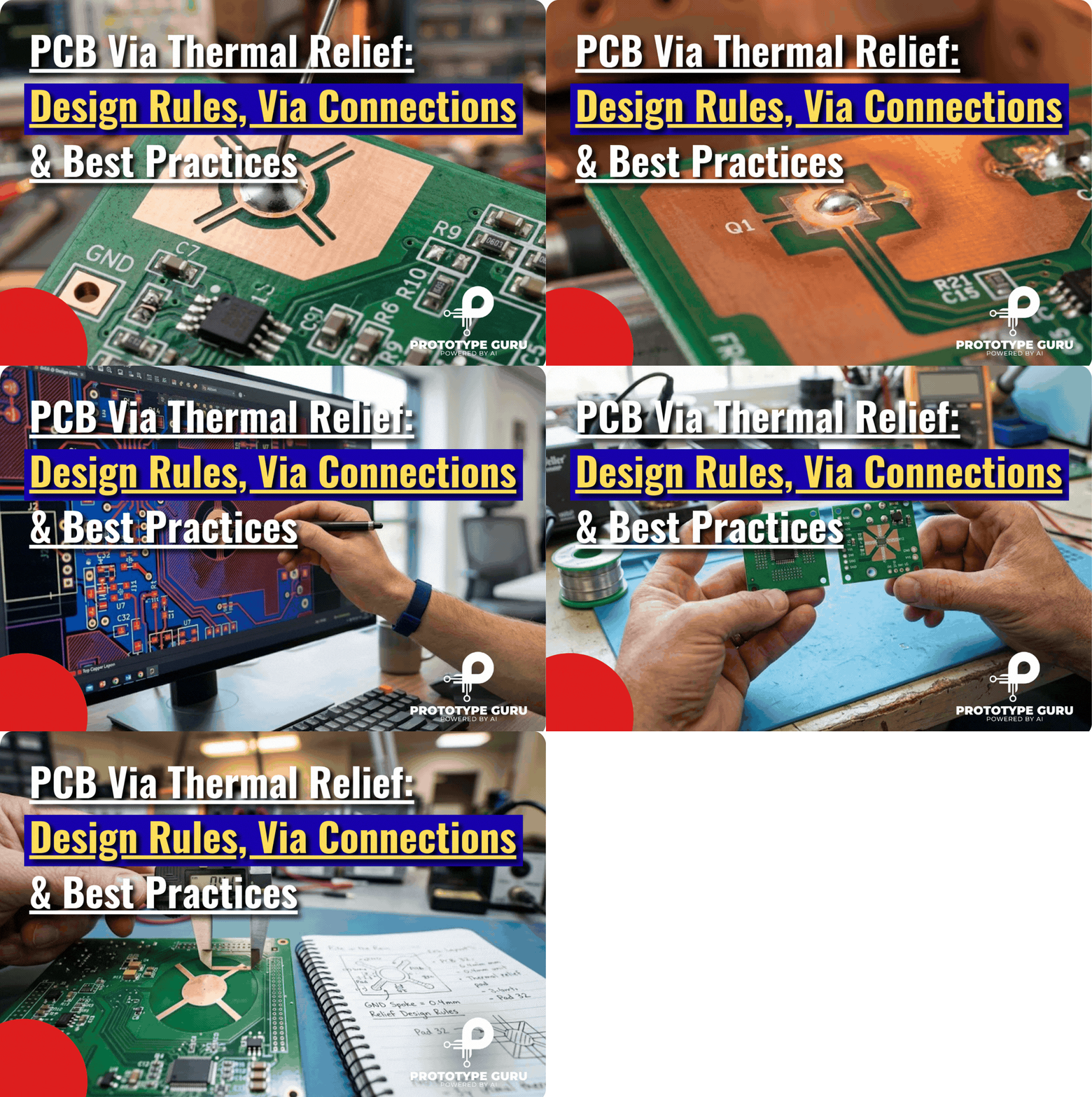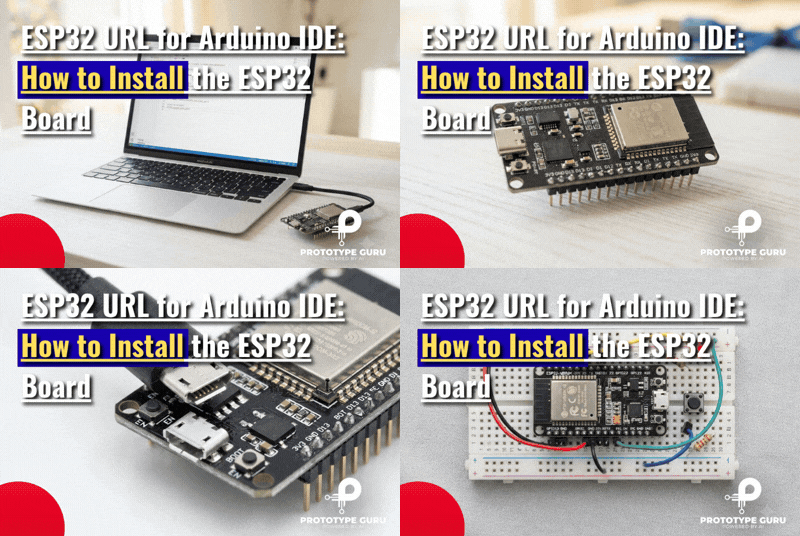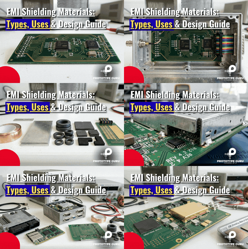













If a via in your ground plane refuses to reach soldering temperature, or a through hole pin produces a dull, grainy joint no matter how long the iron sits on it, the cause is almost always the same: the pad is dumping heat into a large copper plane faster than your iron or reflow oven can replace it. The fix is PCB via thermal relief, a small ring of spokes that controls how quickly heat escapes a pad during soldering while still keeping the electrical and thermal connection intact everywhere else.
I have laid out boards for consumer products, industrial controllers, and a few RF designs where getting this one detail wrong meant reflowing an entire panel a second time. Thermal relief is one of those layout details that rarely gets attention until it causes a problem, which is exactly why it deserves a place in your electronic product design workflow rather than being left to CAD defaults. This guide walks through what PCB via thermal relief actually does, how the spoke geometry works, when to use it versus a solid (flood) connection, and the mistakes that quietly cause the most assembly defects.
What Is PCB Thermal Relief?

Thermal relief is a copper pattern used anywhere a component pad, plated through hole, or via sits inside or touches a large copper plane, such as a ground plane, power plane, or a general copper pour. Instead of connecting the pad to the plane with a solid ring of copper, the design tool breaks the connection into a small number of thin spokes, typically two, three, or four, arranged symmetrically around the pad.
The purpose is straightforward. A large copper plane acts as a heat sink. During reflow or wave soldering, a pad that is solidly flooded into that plane pulls heat away almost as fast as the oven or solder pot can supply it. The pad itself may never reach the melting point of the solder, or it reaches it much later than every other pad on the board. A thermal relief pad slows that heat loss just enough to let the pad and the plane both reach soldering temperature within the normal dwell time.
This is different from a thermal via, which is a dedicated via, or an array of vias, placed under a component specifically to move heat from a hot device into an internal copper plane or the opposite side of the board. Thermal relief and thermal vias solve opposite problems: thermal relief slows heat transfer during soldering, while thermal vias intentionally speed up heat transfer during operation. A board frequently needs both, in different places, for different reasons. If your product design work touches both high power dissipation parts and dense ground planes, it is worth reviewing your circuit board design rules early, before layout starts, rather than patching thermal issues after the first prototype run.
How Thermal Relief Works

Heat always takes the path of least thermal resistance, the same way current takes the path of least electrical resistance. A pad connected directly, with a full solid pour, to a large copper plane has an extremely low thermal resistance path into that plane. Copper is an excellent conductor of heat, so a wide, solid connection lets heat escape the pad almost as quickly as it arrives from the soldering iron tip or the reflow oven’s hot air.
Narrowing that connection down to a small number of spokes increases the thermal resistance of the path without meaningfully increasing the electrical resistance, as long as the spokes are sized correctly. A typical spoke carrying normal signal or low current ground return current is more than adequate electrically even though it looks thin compared to a solid pour. The pad heats up close to the rate it would if it were isolated, reaches soldering temperature within the expected dwell time, and the solder wets properly across the whole pad or barrel.
Cold Solder Joints on Ground Pins
This same principle explains why cold solder joints on ground pins are one of the most common assembly defects reported on boards with dense ground planes. If the copper pour touches the ground pin directly with no relief, the pin is effectively soldering into a heat sink. Reflow profiles are built around typical thermal mass; a directly flooded ground pad falls outside that profile and never fully wets.
Industry Layout Guidance
This exact failure mode is documented well in industry layout guides, including Altium’s thermal relief design guide, which walks through the same cold-joint mechanism from a CAD tool’s perspective.
Simulation Tools
Simulation tools are one of the most reliable ways to confirm a thermal relief pattern is actually working as intended, rather than assuming the CAD tool’s default settings are correct for your stackup and copper weight.
Thermal Imaging
Thermal imaging during first article inspection is another one of the most reliable ways to confirm a thermal relief pattern is actually working as intended, rather than assuming the CAD tool’s default settings are correct for your stackup and copper weight.
PCB Thermal Relief Design Rules
Most CAD tools ship with a default thermal relief rule, but the defaults are rarely optimized for a specific board. IPC-2221, the generic standard for printed board design, addresses thermal relief directly in its section on conductor planes, stating that relief is required for holes subject to soldering in large conductor areas such as ground, voltage, and thermal planes, and that the relief pattern should reduce soldering dwell time by adding thermal resistance during the soldering process, according to the IPC-2221 standard overview.
The table below summarizes the design parameters worth setting deliberately rather than leaving at a tool’s default.
| Parameter | Typical Range | Notes |
|---|---|---|
| Spoke count | 2 to 4 | 4 spokes is the most common default; 2 spokes is used for very small pads |
| Spoke width | 0.25 mm to 0.4 mm (10 to 16 mil) | Must carry the required current per IPC-2152 current tables |
| Spoke angle | 45° (4 spokes) or 90° (2 spokes) | Symmetry keeps thermal load even around the pad |
| Air gap / clearance | 0.2 mm to 0.5 mm (8 to 20 mil) | Set by your fabricator’s minimum clearance and voltage requirements |
| Annular ring | Per class (Class 1, 2, or 3) | See IPC-2221 performance class table |
| Pad-to-plane connection | Thermal relief by default; solid for high current | Override per net where current density demands it |
A few practical notes from board bring up. Fabricators generally want a minimum air gap around any relieved pad so plating and etching tolerances do not accidentally bridge the gap or leave it too wide, both of which affect assembly yield. If your board carries any current-sensitive nets, such as motor drive returns or high power rails, calculate the required trace width per IPC-2152 rather than trusting a default spoke width, since a spoke that is too narrow becomes a resistive hot spot under load, independent of the soldering benefit it provides.
Design rule checks should also flag any pad where thermal relief was applied but the pad sits in a low copper density area. In that case, relief may not be necessary and can be removed, simplifying the fabrication data and slightly improving the mechanical strength of the connection.
Thermal relief rules do not exist in isolation from the rest of your thermal design. Plane stacking, copper weight, and general via placement all interact with how well any single relieved pad performs, and a broader overview like thermal management in PCB design is worth reading before locking in relief-specific rules for a new board.
Thermal Relief on Pads vs Vias
Thermal relief behaves a little differently depending on whether it is applied to a component pad, a standard via, or a dedicated thermal via, and conflating the three is a common source of confusion during design review.
| Feature | SMD / Through Hole Component Pad | Standard Signal Via | Dedicated Thermal Via |
|---|---|---|---|
| Primary purpose | Solder connection to a component | Layer to layer signal routing | Move heat vertically through the board |
| Thermal relief applied | Yes, when touching a plane | Yes, when touching a plane | Rarely, usually solid or tented |
| Soldered during assembly | Yes | Not directly soldered | Not directly soldered |
| Typical spoke count | 3 to 4 | 3 to 4 | N/A, often filled or plated solid |
| Risk if relief is missing | Cold joints, tombstoning | Harder rework, desoldering damage | N/A |
| Risk if relief is present where it should not be | N/A | N/A | Reduced thermal performance, higher junction temperature |
Component pads need relief because they are directly soldered, either by hand, wave, or reflow, and the pad’s ability to reach temperature quickly determines joint quality. Standard vias that pass through a copper plane are usually given relief too, mainly so the board can be reworked or desoldered later without excessive heat sinking making rework difficult or risking pad lifting. This is a detail worth reviewing during any PCB design vs PCB layout discussion with a client, since the two disciplines make different assumptions about where thermal relief belongs.
Dedicated thermal vias, by contrast, exist specifically to move heat away from a hot component into inner layers or the opposite side of the board. Applying thermal relief to these vias defeats their purpose, since the whole point is a low thermal resistance path. Fabricators and design tools typically default to solid, unrelieved, sometimes plugged or filled construction for thermal via arrays under QFN, DFN, and other exposed pad packages, an approach documented in application notes covering heat dissipation through vias in exposed pad packages, such as the one published by ROHM on thermal via heat dissipation.
Thermal Relief Spoke Design
Spoke geometry is where most of the practical engineering judgment happens. The two decisions that matter most are spoke count and spoke width, and both interact with pad size, copper weight, and current requirements.
Spoke Count
Four spokes at 45 degrees is the standard default because it distributes heat and current evenly around a round or square pad. Two spokes at 90 degrees are sometimes used on very small pads where four spokes would leave too little copper area to route reliably. Higher spoke counts, five or more, show up occasionally in high current applications where a single connection needs more aggregate copper cross section while still preserving some thermal isolation, though this is less common and worth validating with your fabricator before committing to a production panel. For a closer look at how these trade-offs play out across different footprint types, Altium’s guide to designing circuit boards with thermal relief pads is a useful companion reference.
Layout Requirements
This trade-off shows up constantly on IoT boards built around exposed-pad modules such as the ESP32, where the module’s thermal pad needs a solid, unrelieved via array while every soldered signal pin around it still needs a correctly sized relief pattern. Our ESP32 selection guide and notes on how to build an IoT prototype quickly both touch on this mixed layout requirement in more detail.
Spoke Width
Spoke width should be sized from the required current, not copied from a template. A rough rule many engineers use as a starting point, and then verify against IPC-2152 current tables for the actual copper weight and expected temperature rise, is to keep total spoke cross sectional area proportional to what a solid trace of similar current rating would need, then distribute that across the number of spokes.
Spoke Length and Clearance
The spoke length is effectively the air gap between the pad and the surrounding copper, and it needs to respect your fabricator’s minimum clearance and any voltage isolation requirements for the net (such as managing ground clearances near RF sections as outlined in a 2.4 GHz PCB antenna design). Longer spokes increase thermal resistance further but also increase electrical resistance and reduce the mechanical strength of the connection, so this is a balance rather than a “longer is always better” parameter.
Antenna and RF layouts add another wrinkle, since spoke geometry can subtly affect ground return path inductance near sensitive feed points. If you are laying out anything working at 2.4 GHz or above, it is worth reviewing spoke placement around ground vias near the antenna feed alongside general 2.4 GHz PCB antenna design guidance rather than treating thermal relief as a purely thermal decision on those specific nets.
When to Use or Avoid Thermal Relief

Thermal relief is not a universal setting. Applying it everywhere, or removing it everywhere, both cause problems. The decision usually comes down to whether the pad will be soldered, whether it needs rework access, and how much current it carries.
Use thermal relief when:
Soldering Method & Plane Connection
The pad is hand soldered, wave soldered, or reflow soldered and connects to a large copper plane
Rework & Desoldering Access
Rework or desoldering access is expected during the product’s life
Current Requirements
The pad’s current requirement is low to moderate and spoke width can comfortably carry it
Heavy Copper Pour
The board uses a heavy copper pour or ground fill across most layers
Consider a solid connection instead when:
Dedicated Thermal Via
The via is a dedicated thermal via meant to move heat out of a hot component
High Current Carrying
The connection carries high current where spoke resistance would create a hot spot or excessive voltage drop
Internal Stitching Via
The pad is not soldered directly, such as an internal stitching via with no assembly step touching it
Mechanical Strength
Mechanical strength of the connection matters more than solderability, such as structural mounting vias
For products destined for regulatory testing, this decision also interacts with certification requirements. Boards headed toward medical device development or industrial product design engineering programs often carry stricter documentation expectations around thermal and current design decisions, which is worth planning for alongside your broader how to certify an electronic product checklist rather than as an afterthought during compliance testing.
Common PCB Thermal Relief Problems
| Problem | Typical Cause | Fix |
|---|---|---|
| Cold solder joints on ground pins | Pad flooded solid into a large plane, no relief applied | Enable thermal relief on the net or override the pad’s plane connection setting |
| Tombstoning on small SMD parts | Uneven heat transfer between the two pads of a two-terminal part | Apply matching thermal relief symmetrically to both pads |
| Excessive voltage drop on a relieved high current pad | Spoke width undersized for actual current | Recalculate spoke width per IPC-2152, or switch to a solid connection for that net |
| Difficult rework or pad lifting during desoldering | No relief on a via or pad embedded in a heavy plane | Add relief, or plan a wider desoldering dwell time and lower iron temperature |
| Reduced thermal performance under a hot component | Thermal relief accidentally applied to dedicated thermal vias | Set thermal via array to solid, unrelieved connection |
| DRC flags on air gap violations | Spoke clearance set below fabricator minimum | Adjust design rule to match the fabricator’s stated minimum air gap |
Most of these issues surface first at first article inspection or during initial assembly bring up, which is exactly the stage where a formal review under PCB testing and inspection procedures catches them before a full production run repeats the same defect across every panel.
For components with genuinely high power dissipation, the fix usually goes beyond relief geometry and into thermal via sizing. Resources such as how thermal vias enhance heat dissipation in PCBs and older but still relevant RF power package guidance like thermal management and mounting methods for surface mount packages go deeper into via array sizing than a relief-only discussion can cover. Small oversights like these rarely get caught until assembly, and repeated respins over the same class of defect are a quieter but real contributor to why hardware startups fail to hit their prototype schedules.
PCB Thermal Relief Best Practices

The checklist below is meant to sit alongside your general PCB layout best practices, not replace them.
- Set spoke width from actual current requirements per IPC-2152, not from a copied template default
- Keep spoke count and angle symmetric around each pad to avoid uneven heat transfer and tombstoning risk
- Use solid, unrelieved connections for dedicated thermal vias under exposed pad packages
- Confirm air gap and clearance values against your fabricator’s minimum before finalizing the design rule
- Review thermal relief settings net by net for any high current or safety critical connections rather than applying one global rule
- Validate the final pattern against IPC-2221 guidance for conductor plane connections before release to fabrication
- Cross check component footprints from your library against the pad’s actual soldering method, since a footprint built for reflow may not need the same relief pattern if the part is later hand soldered in low volume builds
- Inspect a first article board under magnification or thermal imaging before committing to a full panel run
Component selection upstream of layout also affects how much of this matters. A part with a large exposed thermal pad, common in higher power ICs, changes the entire plane connection strategy for that section of the board, which is one more reason thermal relief planning belongs inside your broader electronic component selection guidelines rather than as a separate, late stage layout task.
Frequently Asked Questions
1. What is the difference between a thermal relief pad and a thermal via?
↑2. Does thermal relief weaken the electrical connection to ground?
↓3. How many spokes should a thermal relief pad have?
↓4. Should ground plane vias always use thermal relief?
↓5. Can thermal relief cause tombstoning?
↓6. What spoke width should I use for a high current ground pad?
↓7. Does IPC-2221 require thermal relief?
↓8. Why is my pad not reaching soldering temperature during reflow?
↓Final Recommendations
Treat thermal relief as a net-by-net decision rather than a single global setting. Review it during schematic and stackup planning, not only after layout is complete, and confirm your design rule check settings match your fabricator’s actual clearance and annular ring minimums before releasing files. For boards with mixed requirements, high current power nets next to sensitive low current signals, plan the plane connection strategy for each section separately.