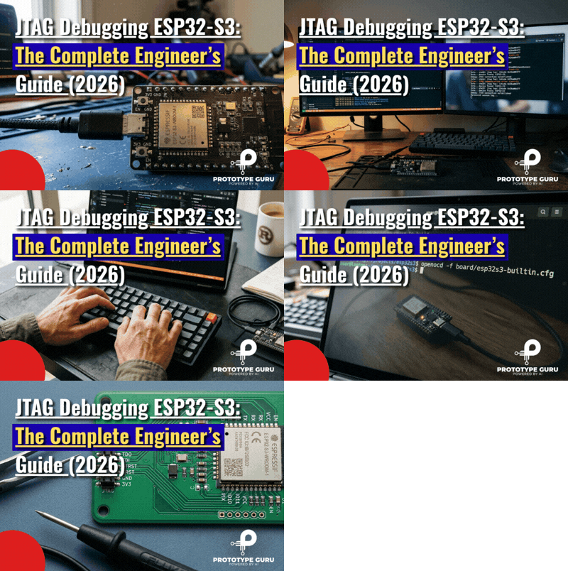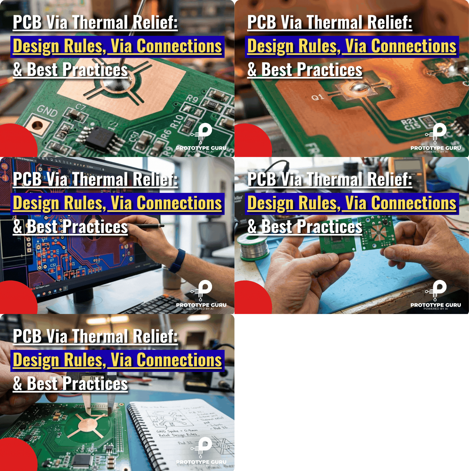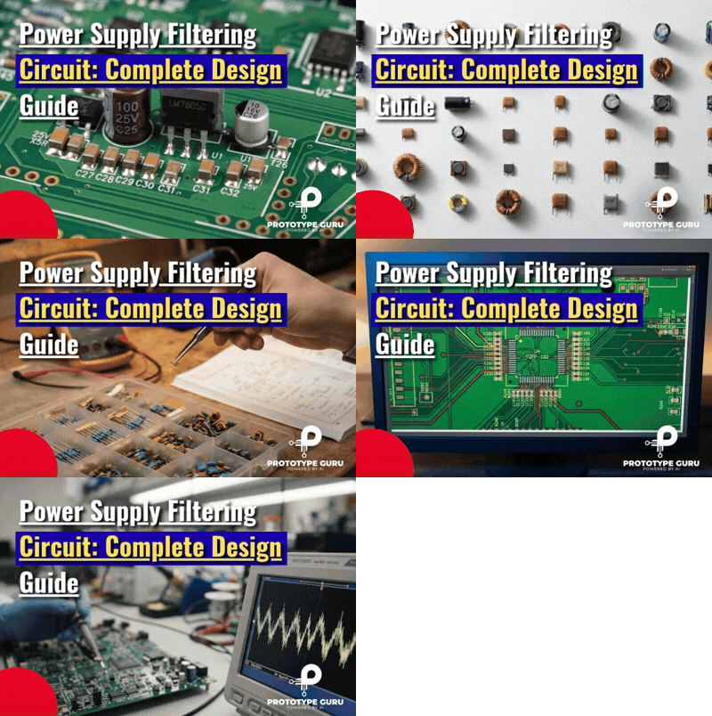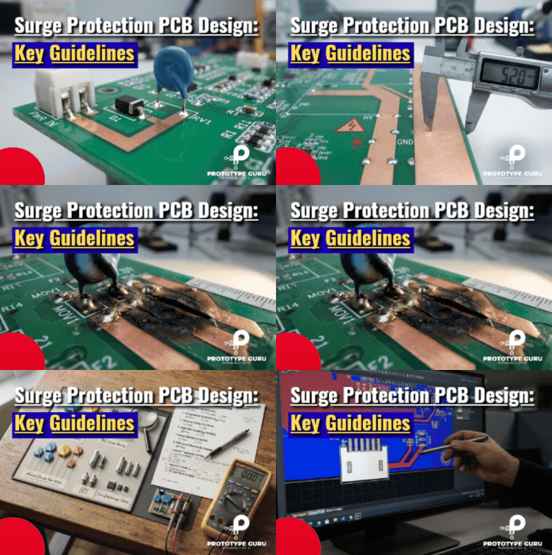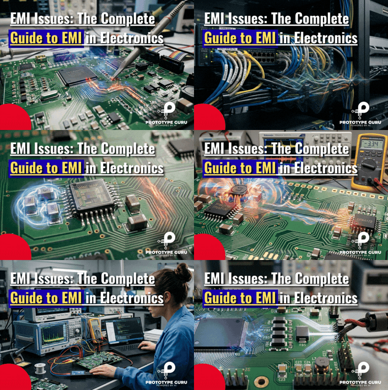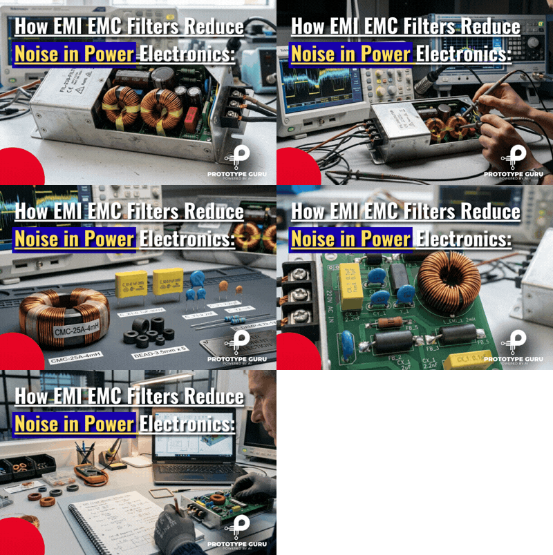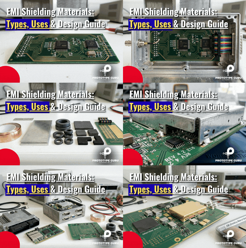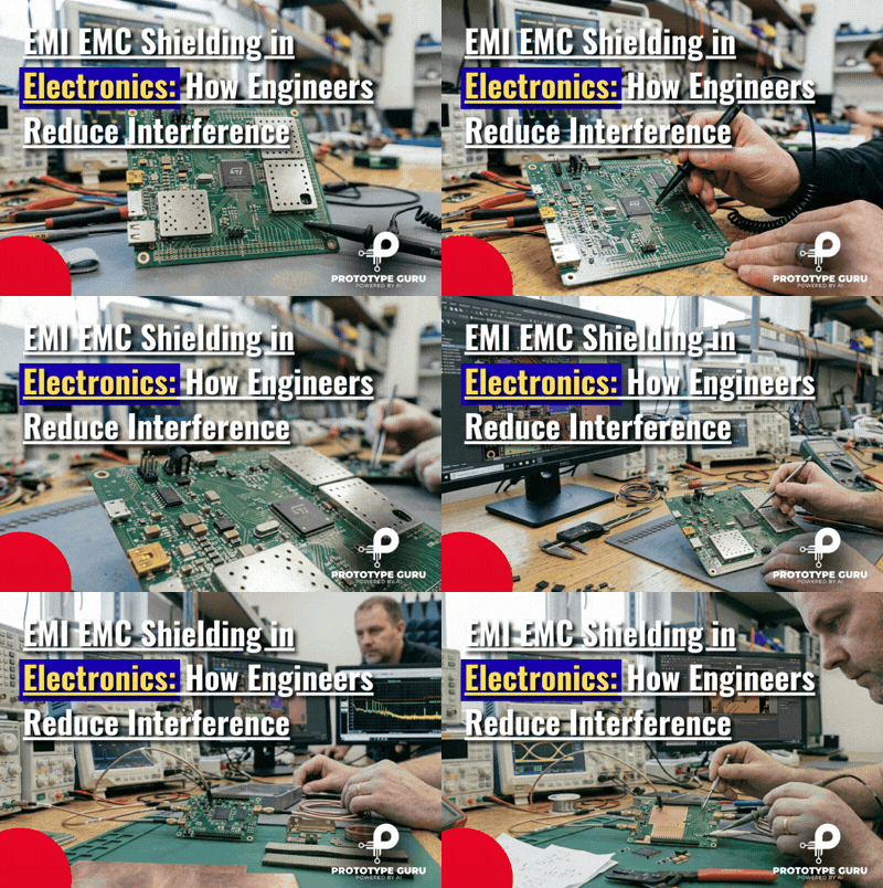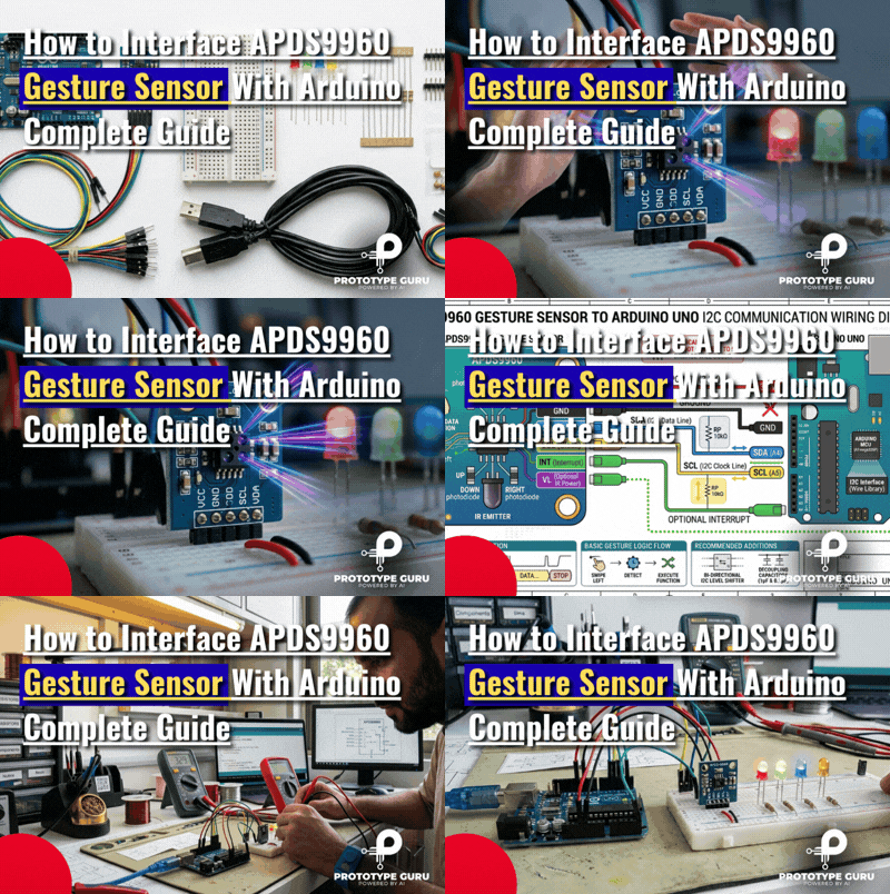









After eight years of debugging noisy rails on everything from wearable sensors to industrial motor controllers, I’ve learned that filtering is rarely the flashy part of a design. Yet it can determine whether an embedded board performs reliably or struggles with interference, signal integrity, and EMC requirements. A well-designed filter helps keep sensitive electronics stable under real-world operating conditions.
This guide explains how to design effective filtering for embedded power rails, from selecting capacitors and inductors to choosing the right filter topology. It also covers component values, frequency behavior, PCB layout, grounding, and common design mistakes. The goal is to help you build cleaner, more stable power delivery and avoid noise problems that can appear during testing or operation.
What Is a Power Supply Filtering Circuit
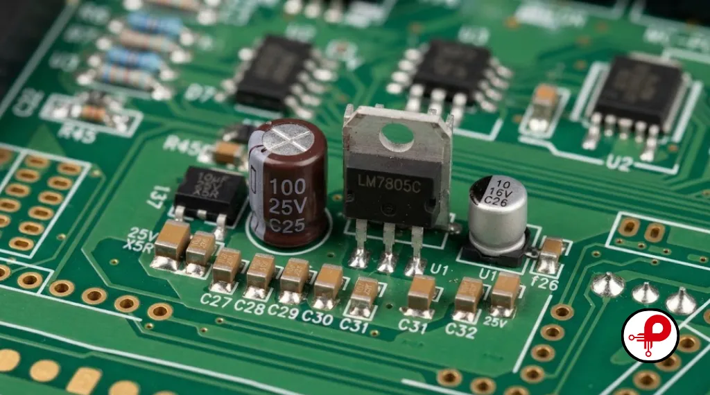
A power supply filtering circuit is a network of passive components, typically capacitors, inductors, and sometimes ferrite beads, placed between a power source and a load to remove unwanted ripple, noise, and transients from the DC voltage rail. The goal is a clean, stable supply voltage that lets sensitive analog and digital circuits operate without glitches, resets, or measurement errors.
In practical terms, filtering happens at three levels: bulk filtering at the input of a regulator, local decoupling at each integrated circuit, and targeted noise suppression for specific frequency bands such as switching harmonics from a buck converter. A well designed filter combines all three, and each layer has a different job.
If you are building a new product from concept to production, this same layered thinking applies across the entire electronic product design workflow, where power integrity decisions made early save significant rework later.
Why Filtering Matters in Modern Electronics
Every power source, whether it is a wall adapter, a battery, or a switching regulator, carries some amount of noise. Linear supplies contribute low frequency ripple from rectification. Switching regulators contribute high frequency harmonics from their switching node. Batteries introduce impedance that changes with state of charge and temperature. Left unfiltered, this noise couples into sensitive nodes and causes real problems.
Common symptoms of poor filtering include:
Microcontroller Resets
Microcontroller resets or brownouts under sudden load transients caused by insufficient local decoupling or excessive supply rail inductance.
ADC Noise Floor
Increased noise floor in analog-to-digital converter readings resulting from power supply ripple or ground bounce coupling into sensitive analog channels.
Audio Circuit Interference
Audible whine, buzz, or interference in audio circuits due to poor power supply rejection ratio (PSRR) or common-mode noise on analog rails.
EMC Compliance Failures
Failed conducted or radiated emissions testing triggered by high-frequency switching noise escaping unshielded cables or improper PCB return paths.
Digital Communication Errors
Communication errors on high-speed digital buses caused by signal integrity degradation, ringing, or impedance mismatches.
Sensor Inaccuracy
Reduced accuracy in sensor and instrumentation circuits stemming from unstable reference voltages or thermal noise coupling.
For teams doing serious electronic hardware design work, power filtering is not an afterthought bolted on before certification. It is planned during schematic capture, validated during prototyping, and confirmed during formal testing before a product ever reaches the market. Poor early planning is one of the quiet reasons behind why hardware startups fail to hit their launch timelines, since a noisy rail discovered late in the program can force a full board respin.
Types of Power Supply Filtering Circuits
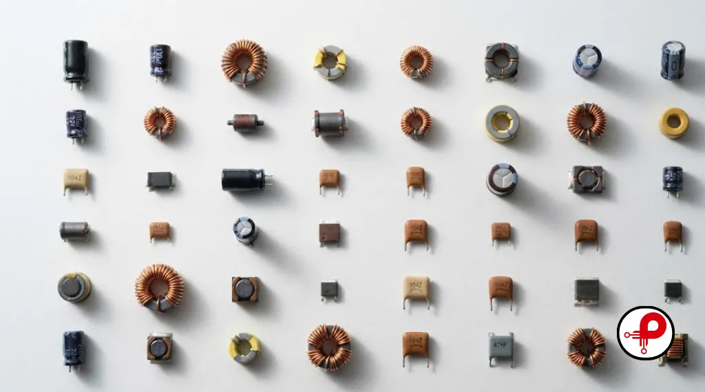
There is no single filter topology that fits every application. The right choice depends on the frequency content you need to suppress, the current the rail carries, and the physical space available on the board.
Bulk Capacitance Filtering
Bulk filtering uses large value electrolytic or polymer capacitors placed close to the input of a regulator or at the point a cable enters the board. Their job is to absorb low frequency ripple and to supply instantaneous current during load transients that a regulator cannot respond to fast enough on its own. Typical values range from tens to thousands of microfarads depending on load current and acceptable ripple.
LC Filters
An inductor placed in series with the rail, paired with a shunt capacitor after it, forms an LC low pass filter. This topology is extremely effective against switching regulator harmonics because the inductor presents high impedance at high frequency while the capacitor shunts remaining noise to ground. LC filters are common on the output of buck converters feeding sensitive analog front ends.
Pi Filters
A pi filter places a capacitor, then an inductor, then another capacitor in sequence, forming a shape that resembles the Greek letter pi. This gives steeper attenuation than a simple LC filter and is often used where a switching supply feeds an RF section or a precision measurement circuit that cannot tolerate switching harmonics.
Ferrite Bead Filtering
Ferrite beads behave like resistors at high frequency while remaining nearly invisible at DC and low frequency. Paired with a small decoupling capacitor, a ferrite bead forms an effective high frequency noise trap that is popular in space constrained designs such as wearables and small IoT sensor nodes, an area covered in more depth in our guide to the development of wearable technology.
Local Decoupling Networks
Every active IC needs its own local decoupling, usually a combination of a small ceramic capacitor for high frequency transients and a slightly larger ceramic or tantalum capacitor for mid frequency support. This is not optional bulk filtering, it is a distributed network placed within millimeters of each power pin.
Component Selection for Effective Filtering
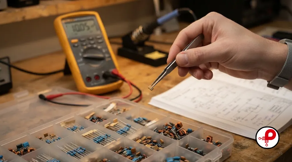
Choosing the right components is where theory meets the realities of cost, size, and supply chain. Following solid electronic component selection guidelines prevents a design from being over engineered in one area while remaining vulnerable in another.
Capacitor selection checklist:
Capacitor Selection Best Practices
Dielectric Type Matching
Match dielectric type to the job: use X7R or X5R ceramics for general decoupling, and C0G or NP0 for precision analog nodes.
Voltage Rating Margin
Verify that the voltage rating includes proper margin, typically 1.5 to 2 times the working voltage for ceramic options.
Ripple Current & ESR
Confirm that the equivalent series resistance (ESR) is low enough to handle the expected ripple current without excessive heating.
Polymer Alternatives
Consider polymer capacitors where low ESR and long operating life are required in place of standard electrolytics.
Inductor selection checklist:
Inductor Selection Best Practices
Saturation Current Rating
Confirm that the saturation current rating exceeds the peak load current with proper safety margin to avoid sudden inductance collapse.
DC Resistance & Thermal Rise
Check DC resistance against acceptable voltage drop limitations and expected thermal rise under continuous operating loads.
Self-Resonant Frequency
Review the self-resonant frequency (SRF) to ensure the inductor still behaves inductively at the specific noise frequency you are targeting.
Magnetic Shielding
Choose shielded inductors near sensitive analog or RF sections to significantly reduce radiated magnetic field coupling and EMI.
For RF adjacent designs, filtering interacts closely with antenna performance, and teams working on connected products often reference our notes on 2.4 GHz PCB antenna design alongside their power filtering strategy, since a noisy rail can desensitize a nearby receiver front end.
PCB Layout Best Practices for Filtering Circuits
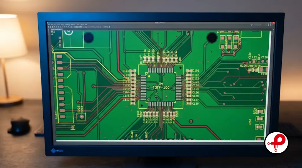
A correctly chosen filter can still fail if the layout undermines it. Layout is where many teams lose the benefit of good component selection, and it is one of the clearest differences between PCB design and PCB layout as distinct disciplines within the same project.
Layout guidelines that consistently work:
- Place decoupling capacitors as close as physically possible to the IC power pin, with the shortest possible trace to both the pin and the ground return
- Use dedicated ground pours under filter networks rather than routing ground as a thin trace
- Keep the high current loop of an LC or pi filter as small as possible to minimize radiated loop area
- Separate noisy switching regulator sections from sensitive analog sections with a physical and, where possible, a plane level barrier
- Route the noisy switch node of a regulator away from other signal traces, and keep it short and direct
- Use multiple vias for ground connections on filter components to lower return path inductance
- Avoid placing filter inductors directly over digital signal layers where magnetic coupling can inject noise
These principles are part of our broader PCB layout best practices guidance and connect directly to the general circuit board design rules that govern trace width, spacing, and plane stitching across an entire board.
Common Mistakes and Troubleshooting
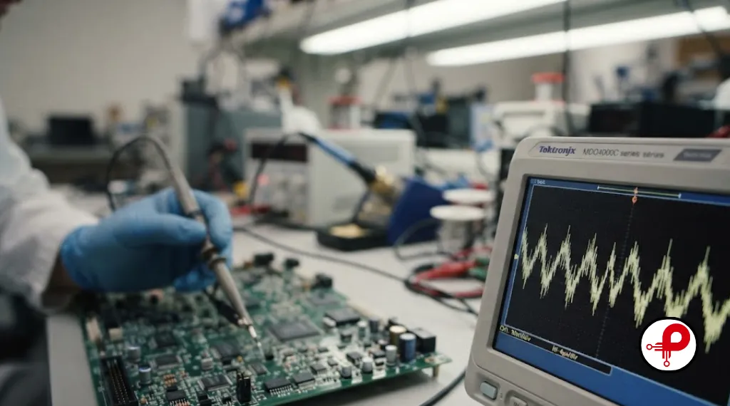
Even experienced designers repeat a handful of filtering mistakes. Recognizing them early saves a redesign cycle.
Frequent mistakes:
- Relying on a single bulk capacitor instead of a distributed decoupling network
- Placing decoupling capacitors on the wrong side of a via with high inductance in the return path
- Choosing a ceramic capacitor value that collapses under DC bias, leaving far less effective capacitance than expected
- Ignoring ESR at the specific ripple frequency, which allows more ripple through than the datasheet capacitance would suggest
- Forgetting thermal effects, since electrolytic capacitor ESR rises significantly at low temperature
- Skipping bench validation with an oscilloscope before committing to production tooling
Troubleshooting workflow when a rail is noisy:
- Probe directly at the load pin with a short ground spring, not a long ground lead, to avoid measurement artifacts
- Compare ripple with the load active versus idle to isolate whether noise is load dependent
- Use a spectrum view or FFT on the oscilloscope to identify the dominant noise frequency
- Add a small ferrite bead and observe whether high frequency content drops, which confirms a high frequency noise source
- Check for shared ground paths between noisy and sensitive sections that may be injecting common mode noise
If a design is heading toward regulatory submission, catching these issues before formal testing avoids costly delays, and our page on PCB testing and inspection outlines the verification steps we recommend before a board goes to certification.
Real World Case Study

On a recent industrial sensor project, a customer reported intermittent analog to digital converter errors that only appeared when a nearby motor driver was active. The board had a single bulk capacitor at the regulator input and minimal local decoupling. We added a two stage filter: a small ferrite bead followed by a local ceramic capacitor right at the analog to digital converter reference pin, combined with tightening the ground return path in layout. Ripple at the reference pin dropped from over 40 millivolts peak to under 3 millivolts, and the reported errors disappeared entirely. This kind of targeted fix is common in industrial product design engineering, where electrically noisy environments make filtering a first class design requirement rather than an afterthought.
A similar pattern shows up in connected sensor nodes built around modules such as the ESP32, where radio transmit bursts pull sudden current from the rail. Our ESP32 selection guide covers how supply transient response interacts with radio performance on these modules, and the filtering approach described above applies directly to that class of design.
Comparison Table of Filter Types
| Filter Type | Best Use Case | Frequency Range | Relative Cost | Board Space |
|---|---|---|---|---|
| Bulk Capacitance | Load transient support, low frequency ripple | Below 1 kHz | Low | Moderate |
| LC Filter | Switching regulator harmonic suppression | 100 kHz to 10 MHz | Moderate | Moderate |
| Pi Filter | RF or precision analog supplies | 1 MHz to 100 MHz | Moderate to high | Higher |
| Ferrite Bead plus Capacitor | High frequency noise, compact designs | 10 MHz and above | Low | Small |
| Local Decoupling Network | Every active IC power pin | Broadband | Low | Minimal |
Quick Decision Guide
Use bulk capacitance when the load draws large, fast current steps. Use an LC filter when a switching regulator feeds an analog or RF section. Use a ferrite bead network when board space is limited and only high frequency noise needs suppression. Use a pi filter when a design must meet strict RF or precision measurement requirements and simple LC filtering is not enough.
This same structured decision process applies broadly to teams moving through product development and into rapid prototyping, where early filter decisions are validated on the first prototype run rather than discovered during compliance testing. Getting this right early also matters for regulated products, since our overview of how to certify an electronic product explains how conducted emissions testing directly reflects the quality of a board’s power filtering.
Frequently Asked Questions
1. What is the comprehensive purpose of a power supply filtering circuit?
↑2. What is the fundamental difference between decoupling and filtering?
↓3. Why does my microcontroller experience sudden resets under high load transients?
↓4. How close and how layout-conscious should decoupling capacitors be relative to an IC?
↓5. Can I simply use one large bulk capacitor instead of combining several smaller values?
↓6. Which capacitor dielectrics are optimal for power supply filtering applications?
↓7. Do ferrite beads offer any effective filtering benefits at direct current (DC)?
↓8. What is the most reliable procedure to verify if a power filter is performing correctly?
↓Key Takeaways
A power supply filtering circuit combines bulk capacitance, targeted LC or pi filtering, and local decoupling to deliver a clean, stable rail. Component selection must account for real world behavior such as DC bias derating and ESR at the actual ripple frequency, not just the nominal datasheet value. Layout discipline, particularly short ground return paths and tight component placement, often determines whether a well chosen filter actually performs as designed.
Final Recommendations
Start filter planning during schematic capture, not during layout cleanup. Validate every rail with an oscilloscope under real load conditions before moving to production. Treat filtering as a system level concern that touches component selection, embedded systems development, and mechanical enclosure design together, since shielding and grounding choices in the enclosure can influence how effective a filter is in practice.
Related Services
Teams looking for hands on support with rail design, prototyping, or pre certification validation can explore our PCB design services, rapid prototyping support, and IoT development work, alongside our experience in medical device development where power supply cleanliness is a strict regulatory requirement.
Call to Action
If your board is showing unexplained resets, noisy measurements, or failed emissions tests, the root cause is often the power supply filtering network. Reach out to our engineering team for a design review before your next prototype run, and let us help you get a clean, certifiable rail on the first pass instead of the third.
For general background on component behavior referenced throughout this guide, industry documentation from Texas Instruments, Analog Devices, Microchip, STMicroelectronics, and the IEEE provides additional depth on capacitor dielectric behavior, inductor saturation characteristics, and EMC test methodology.