


Written from the perspective of a practicing electronics engineer with eight-plus years of hands-on PCB design and manufacturing experience. Verified against IPC, NASA workmanship, and Texas Instruments documentation. Last updated for PrototypeGuru readers.
I still remember the first board I sent to fabrication with the wrong assumption baked in. I had specified through-hole connectors on a board that also carried a dense BGA processor, without thinking through how the two would actually get soldered on the same production line. The board worked, eventually, but the extra wave soldering pass and the hand touch up it required added a week to the schedule and a real dent in the budget. That’s the kind of lesson that sticks, and it’s exactly why the SMT vs through-hole decision deserves more thought than most beginner guides give it.
This guide walks through what actually separates surface mount technology from through-hole technology, where each one genuinely earns its place on a board, and how experienced teams decide between them, or combine both, on real products.
What Is SMT and Through-Hole Technology?
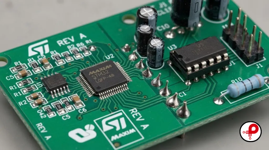
Quick answer: SMT (surface mount technology) mounts components directly onto pads on the surface of a PCB using solder paste and reflow soldering, while through-hole technology (THT) inserts component leads into drilled holes and solders them on the opposite side of the board. SMT enables smaller, denser, automated assembly. THT provides stronger mechanical joints and easier manual rework.
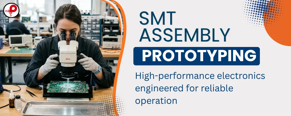
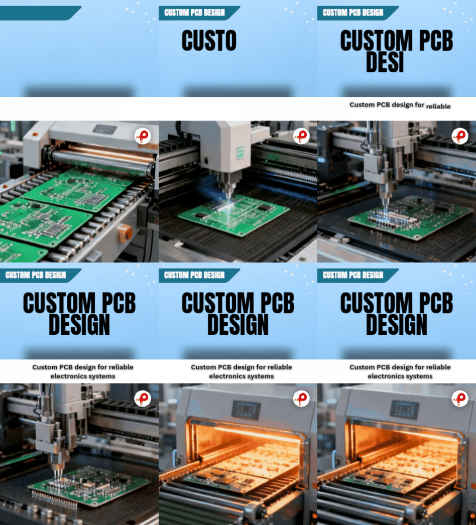
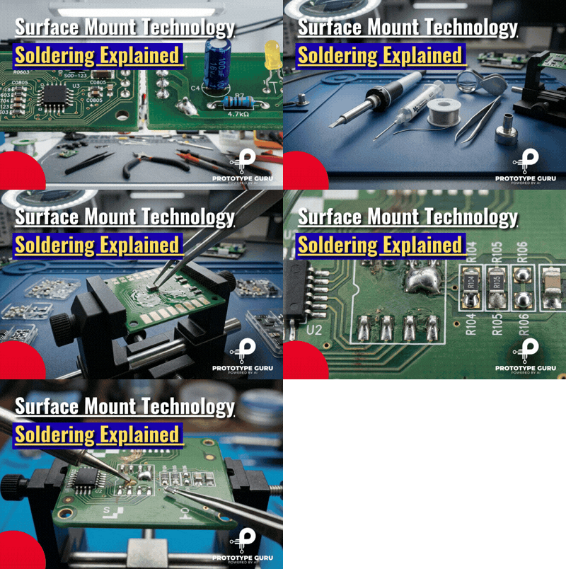
Surface mount technology places components, often called SMDs, flat against copper pads on the board surface. There’s no drilling involved for the component itself. Solder paste is printed onto the pads, the part is placed by an automated pick and place machine, and the whole board passes through a reflow oven that melts the paste into a permanent joint.
Through-hole technology is the older of the two approaches. Component leads pass through drilled, plated holes and are soldered on the reverse side, either by hand or through a wave soldering machine that flows molten solder across the underside of the board. According to Wikipedia’s technical overview of through-hole technology, the mechanical bond formed when a lead passes through and anchors within the board gives noticeably better resistance to vibration and mechanical shock than a surface-only joint, which is exactly why it’s genuinely still in active use, not a legacy method kept alive out of nostalgia. Anyone who has read our piece on why hardware startups fail knows that picking the wrong manufacturing approach early on is one of the quieter ways a promising product stalls out before it ever reaches customers.
Understanding this distinction matters before you even open your layout tool, since it shapes decisions covered in our broader guide on PCB design versus PCB layout: the mounting technology you choose influences footprint selection, stackup, and drill requirements from the very first schematic decision onward.
SMT vs Through-Hole: Key Differences
At a glance, the differences come down to five things: size, strength, automation, repairability, and cost structure.
| Factor | SMT | Through-Hole |
|---|---|---|
| Component size | Small, compact footprints | Larger, bulkier packages |
| Board density | High, both sides usable | Lower, holes limit routing |
| Mechanical strength | Weaker, solder-only bond | Strong, lead passes through board |
| Assembly speed | Fast, fully automated | Slower, often manual insertion |
| Rework and repair | Difficult, needs hot air tools | Easier, accessible with basic tools |
| Typical cost at volume | Lower per unit at scale | Higher labor cost at scale |
| Best for high frequency signals | Better, shorter lead inductance | Weaker above roughly 100 MHz |
| Vibration and shock resistance | Lower | Higher |
That last row matters more than it might look at first glance. If you’re designing anything destined for industrial product environments, vibration and thermal cycling aren’t theoretical concerns, they’re the reason certain connectors and power components still ship through-hole even on an otherwise fully SMT board.
According to IPC, the global standard IPC-A-610 covers acceptance criteria for both surface-mount and through-hole solder joints under a shared framework of Class 1, 2, and 3 product categories, with Class 3 reserved for high-performance and harsh-environment products. That framework alone tells you something useful: the industry doesn’t treat one method as universally superior. It treats them as tools suited to different reliability requirements.
SMT vs Through-Hole Assembly Process
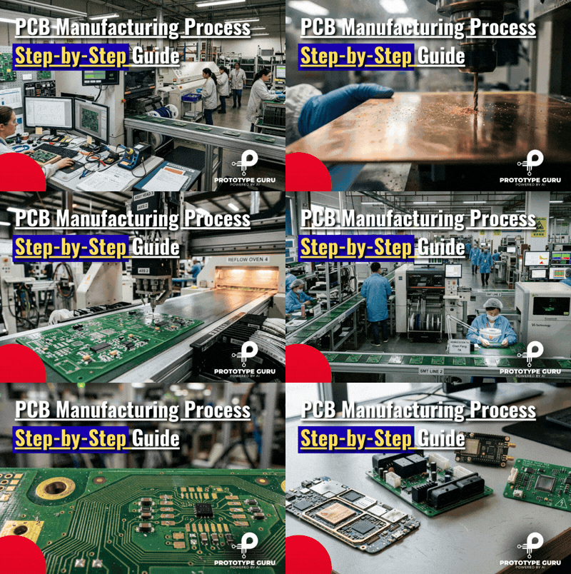
The assembly process itself is where the practical differences become obvious on the factory floor.
How SMT Assembly Works
1. Solder Paste Printing
Solder paste is printed onto the board through a stencil aligned to the pad layout.
2. Component Placement
A pick and place machine positions each component onto its wet paste pads.
3. Reflow Soldering
The populated board passes through a reflow oven, where controlled heating melts the paste and forms the joint as it cools.
4. Automated Optical Inspection
Automated optical inspection checks for missing, shifted, or poorly soldered parts.
A single modern pick and place line can place tens of thousands of components per hour, which is the main reason SMT dominates high-volume consumer electronics. According to Texas Instruments, reflow and wave soldering each require specific temperature profiles matched to component moisture sensitivity ratings, and getting that profile wrong is one of the more common causes of hidden solder defects on otherwise well-designed boards.
How Through-Hole Assembly Works
1. Hole Drilling
Precisely sized holes are drilled through the board at each component’s lead pattern.
2. Component Insertion
Leads are inserted, either by a hand operator or an automated insertion machine.
3. Soldering
The board passes over a wave soldering machine, or is hand soldered, forming joints on the underside.
4. Trimming and Inspection
Leads are trimmed and joints are visually inspected.
According to NASA’s own workmanship standards, through-hole components with significant mass, generally above about 7 grams total or 3.5 grams per lead, require additional mechanical securing beyond the solder joint itself, and heat-producing parts dissipating a watt or more need a standoff of at least 1.5 millimeters from the board surface. That’s a level of mechanical detail SMT components rarely need to worry about, and it’s a good example of why through-hole still earns its place on boards that have to survive real physical stress.
If your board mixes technologies, our guide on PCB testing and inspection covers how inspection strategy has to adapt depending on which joints are hidden underneath a package versus visually accessible on a through-hole lead.
SMT vs Through-Hole: Cost, Size and Manufacturing
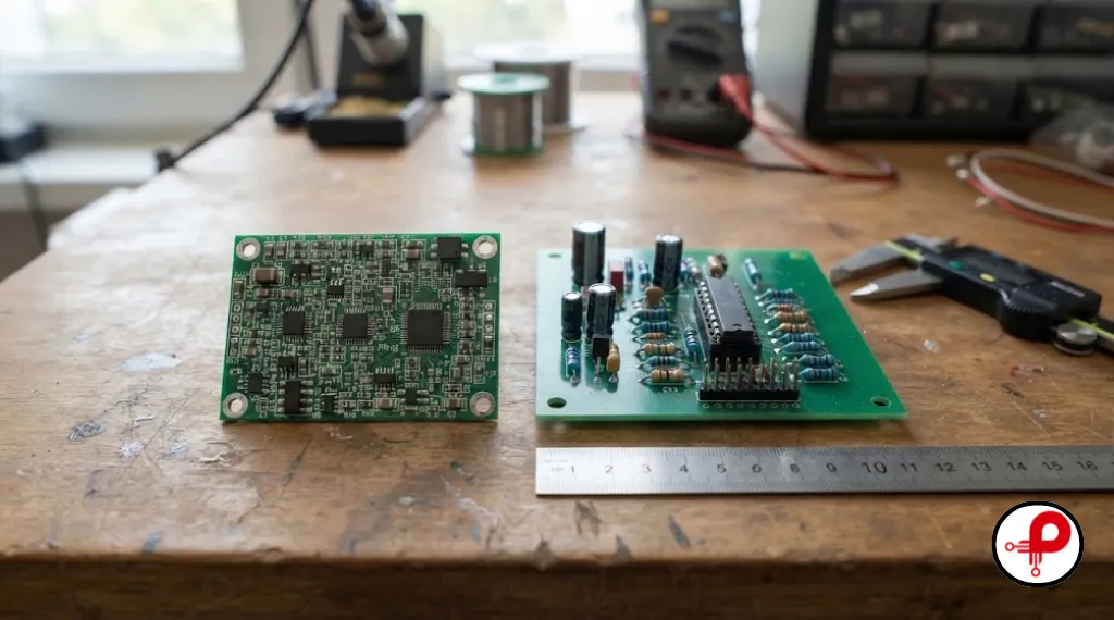
Cost comparisons between SMT and through-hole rarely come down to a single number, since fabrication cost, assembly labor, and long-term rework cost all pull in different directions.
On the fabrication side, through-hole boards cost more to drill, particularly on high pin count connectors or dense header arrays, since every hole is a discrete manufacturing step. SMT boards skip most of that drilling entirely for the components themselves, though vias for routing still require holes of their own, just far smaller ones.
On the assembly side, SMT wins decisively at volume. Automated placement and reflow soldering scale efficiently, while through-hole insertion, especially for non-standard connectors, often still needs a human hand somewhere in the process. That labor cost compounds across a production run in a way that a single prototype board never reveals.
Where through-hole tends to claw cost back is in low volume runs, rework-heavy development cycles, and field repair. A blown through-hole component on a board out in the field can often be replaced with a soldering iron and a spare part. An SMT rework of the same fault usually needs a hot air station, steady hands, and considerably more time. This is exactly why our guide to building an IoT prototype quickly leans on through-hole and mixed boards for early hardware iterations, even when the final production design will be almost entirely SMT.
Component density is the other side of this equation. Following solid circuit board design rules and PCB layout best practices, SMT lets you place far more components in the same board area, and populate both sides, which is often the deciding factor for compact products regardless of what the cost comparison alone would suggest.
Manufacturing speed compounds this further at scale. A well-tuned SMT line can move a completed board through placement and reflow in a matter of minutes, while a board with a meaningful number of through-hole parts often has insertion, wave soldering, lead trimming, and manual touch-up as separate, sequential steps. On a run of a few hundred boards that difference barely registers. On a run of tens of thousands, it becomes the dominant line item in your assembly quote, which is exactly why volume forecasts belong in the SMT versus through-hole conversation from the very first design review, not after the first production quote comes back higher than expected.
Advantages and Limitations of SMT
SMT’s strengths are well documented, but the limitations matter just as much when you’re the one signing off on a design.
| Advantages | Limitations |
|---|---|
| Strong mechanical bond, since the lead physically passes through the board and anchors the joint | Larger footprint, limiting component density |
| Far easier manual rework and field repair with basic tools | Slower assembly, often requiring manual insertion or dedicated insertion machinery |
| Better tolerance for vibration, mechanical shock, and thermal cycling | Additional PCB fabrication cost from drilling |
| Well suited to prototyping, since components are easy to swap by hand during development | Higher labor cost per unit at production volume |
| The practical choice for electromechanical parts: connectors, relays, switches, fuses, and battery holders | Components generally sit on one side of the board only |
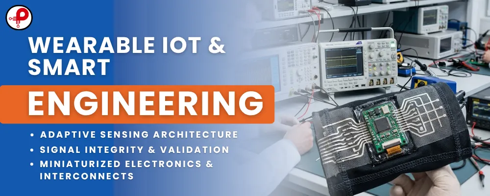
This tradeoff is exactly why applications like wearable technology development lean almost entirely on SMT. Space is the dominant constraint in a wearable, and the mechanical stress that would concern an industrial engineer is usually manageable through good enclosure design instead of the PCB assembly method itself.
Advantages and Limitations of Through-Hole Technology
Through-hole technology often gets framed as outdated, which undersells how deliberately it’s still specified on real products.
| Advantages | Limitations |
|---|---|
| Strong mechanical bond, since the lead physically passes through the board and anchors the joint | Larger footprint, limiting component density |
| Far easier manual rework and field repair with basic tools | Slower assembly, often requiring manual insertion or dedicated insertion machinery |
| Better tolerance for vibration, mechanical shock, and thermal cycling | Additional PCB fabrication cost from drilling |
| Well suited to prototyping, since components are easy to swap by hand during development | Higher labor cost per unit at production volume |
| The practical choice for electromechanical parts: connectors, relays, switches, fuses, and battery holders | Components generally sit on one side of the board only |
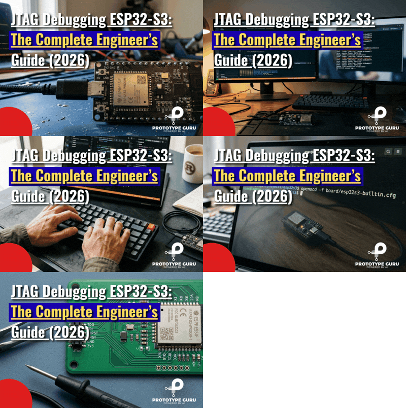
This is precisely why a JTAG debugging setup on an ESP32-S3 almost always uses a through-hole pin header for the debug connector itself, even though the ESP32-S3 module driving the board is a dense SMT part. You need something a debug probe cable can physically grip and reconnect to repeatedly, and a surface mount pad simply isn’t built for that kind of repeated mechanical connection.
When Should You Use SMT or Through-Hole?
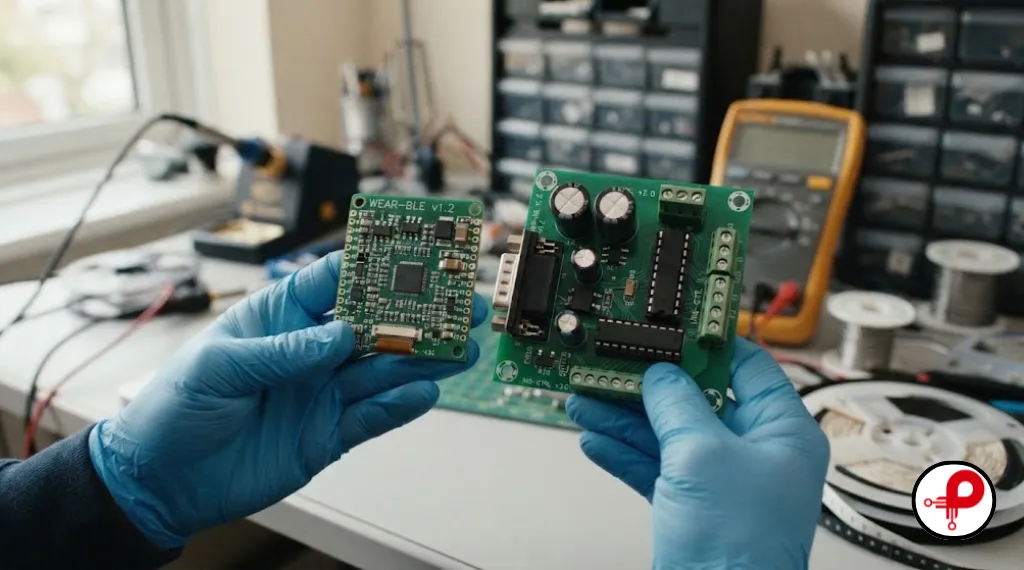
Most real engineering decisions come down to matching the mounting technology to what the product actually has to survive and how many units you’re building.
Use this as a starting checklist rather than a rigid rule:
- Choose SMT when the design needs high component density, the product will be manufactured at meaningful volume, high frequency or high speed signals are involved, or board size is a hard constraint.
- Choose through-hole when the part is electromechanical, the board will see significant vibration or shock, the component needs to survive frequent field repair, or you’re still in early prototyping and expect to swap parts by hand.
- Choose mixed technology when most of the board is dense digital logic best served by SMT, but a handful of connectors, power components, or user-facing parts genuinely need the mechanical strength of through-hole.
A few concrete, real-world examples make this easier to apply than the abstract version:
An ESP32 module selection for a connected product is almost always SMT, since the module itself is a dense, pre-certified surface mount part, and there’s no practical through-hole equivalent at that level of integration.
A 2.4 GHz PCB antenna design leans on SMT for the same reason the comparison table above flags high frequency performance: shorter SMT lead lengths reduce parasitic inductance that would otherwise detune an RF matching network far more than it would affect a simple digital signal.
A medical device intended for repeated sterilization cycles or drop resistance often specifies through-hole for its battery connector and external I/O, even while the internal signal processing sits on a dense SMT board, precisely because that connector needs to survive mechanical stress the rest of the board never sees.
Following a structured electronic product design workflow usually means making this SMT versus through-hole call separately for each functional block on the board, rather than picking one technology for the entire design up front.
Can SMT and Through-Hole Be Used Together?
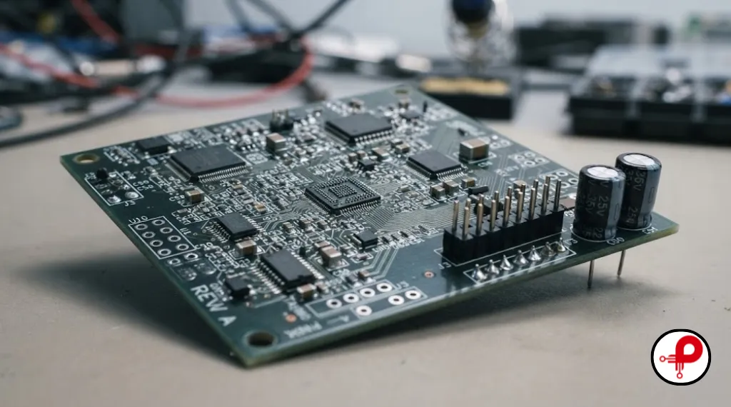
Yes, and on real production boards, this is the norm rather than the exception.
Mixed technology assembly combines SMT and through-hole components on the same board, most commonly with SMT parts handling the dense digital logic and through-hole reserved for connectors, large electrolytic capacitors, and anything electromechanical. In a typical mixed assembly process, SMT components are placed and reflow soldered first, then through-hole components are inserted and wave soldered or hand soldered afterward, since reflow temperatures would damage components that go through afterward if the order were reversed.
This approach directly supports the design-for-testability considerations covered in our guide on PCB design for testability: through-hole test points and headers remain some of the easiest, most reliable places to gain physical probe access on an otherwise dense SMT board, which is exactly why so many mixed boards keep at least a few through-hole test points even when nothing else on the board strictly requires them.
Mixed technology also touches your thermal design more than most engineers expect going in. Our PCB thermal relief design rules guide covers how through-hole pads tied into large copper pours need different relief patterns than SMT pads, since wave soldering heat transfer behaves differently from reflow, and getting that wrong on a mixed board is a common, avoidable source of cold solder joints.
If your product needs to pass formal environmental or safety testing, our guide on how to certify an electronic product is worth reading before you finalize which components go on which technology, since certification bodies often care specifically about the mechanical reliability of exactly the connectors and power components this section describes.
Component selection deserves the same deliberate treatment. Our electronic component selection guidelines walk through how to evaluate whether a given part is genuinely better suited to SMT or through-hole for your specific application, rather than defaulting to whatever package happens to be easiest to source.
Frequently Asked Questions
1. Is SMT better than through-hole?
↑2. Can you hand solder SMT components?
↓3. Why do through-hole components still exist if SMT is smaller and cheaper at scale?
↓4. What is mixed technology PCB assembly?
↓5. Does SMT or through-hole affect PCB signal integrity?
↓6. Is through-hole considered obsolete?
↓7. Which is easier for beginners and hobbyists?
↓8. When should you choose one over the other in a design?
↓Getting the SMT versus through-hole decision right early saves far more time than it costs. The mistake I made on that first board wasn’t choosing through-hole connectors, it was not thinking through how that choice would interact with the rest of the assembly process until the board was already at the fabricator. Treat the decision the way you’d treat any other engineering tradeoff: component by component, weighed against what that specific part actually has to survive, rather than picking one technology and forcing the whole board to follow it.
Key takeaways:
- SMT wins on density, automation, cost at volume, and high frequency signal performance.
- Through-hole wins on mechanical strength, field repairability, and tolerance for vibration and shock.
- Most real production boards use both, with SMT handling dense digital logic and through-hole reserved for connectors and electromechanical parts.
- The decision belongs at the component level, not the board level. Ask what each specific part has to survive before defaulting to whichever package is easiest to source.
- Standards bodies like IPC and NASA don’t treat either method as universally superior, they define acceptance criteria for both because both remain in active, deliberate use across the industry.
If you’re working through this decision on an active design and want a second set of eyes on your component mix, our team at PrototypeGuru works through exactly this kind of layout and manufacturing tradeoff daily, and we’re glad to take a look at what you’re building.
Disclaimer: This article reflects general engineering guidance current at the time of writing. Always confirm specific soldering, drilling, and mechanical requirements against your contract manufacturer’s own process documentation and the current revision of any referenced standard before finalizing a production design.