











Battery life complaints are almost never a “software problem” or a “battery problem.” Nine times out of ten, when I get pulled into a product that’s draining its coin cell in three weeks instead of three years, the root cause traces back to decisions made at the schematic and layout stage; decisions nobody flagged as power-related at the time. After eight years of taking embedded boards from prototype to certified production, I’ve learned that low power circuit design isn’t a checklist you run once before tape-out. It’s a mindset that has to run through every layer, from transistor selection to firmware sleep states.
This guide walks through what actually moves the needle in low power circuit design; not textbook theory, but the techniques, tradeoffs, and mistakes I see repeatedly on real boards.
What Is Low Power Circuit Design?
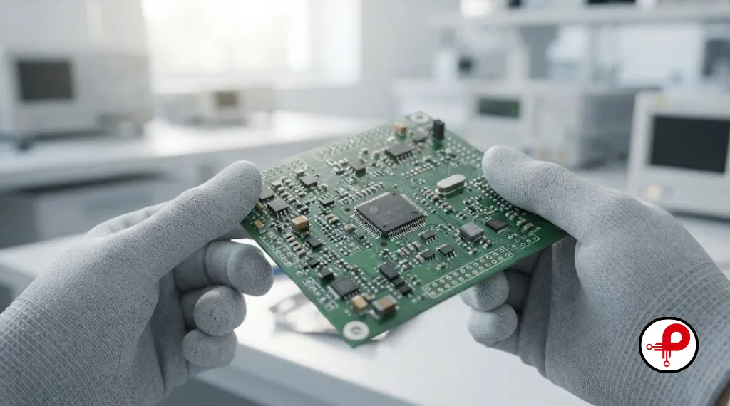
Low power circuit design is the practice of engineering electronic circuits, at the transistor, IC, and board level, to minimize energy consumption while still meeting performance, area, and cost targets. It combines techniques such as supply voltage scaling, clock and power gating, transistor sizing, multi-threshold voltage design, and duty cycling to reduce both dynamic power (consumed while switching) and static/leakage power (consumed while idle).
Unlike general “power management,” low power circuit design starts at the architecture and schematic level, not just in firmware. A perfectly written sleep-mode driver cannot fix a regulator that was sized wrong or a microcontroller selected without checking its leakage current at your target temperature.
Who Needs This
If you’re designing wearables, IoT sensor nodes, implantable medical devices, remote monitoring equipment, or anything running on a coin cell or energy harvester, low power circuit design isn’t optional; it’s the primary design constraint, often more important than raw performance. Teams building wearable technology in particular live or die by milliamp-hours.
Why Low Power Design Matters in 2026
Three forces are pushing power efficiency higher on every engineering priority list right now:
Power Consumption Variance
Two boards built from the identical schematic and BOM can have significant current draw differences purely from layout parasitic effects and unmanaged node switching.
Battery Drain Surprises
A device that passes bench testing can still fail battery life targets because of hidden wake-up transients, floating GPIO states, or unoptimized sleep currents.
Thermal & Power Limits
System reliability is often limited by thermal dissipation bottlenecks and poor regulator choices long before it is limited by the silicon’s theoretical capabilities.
I’ve also noticed a quieter shift: customers now expect “always-on” convenience, voice wake words, background sensing, continuous BLE advertising, on the same battery life they had five years ago without any of that. That gap only closes through disciplined low power circuit design, not bigger batteries.
Understanding Power Consumption: Dynamic, Static, and Leakage Power
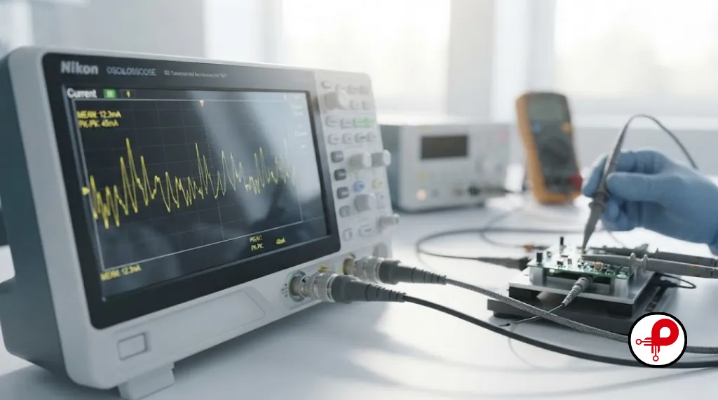
Before touching any technique, you need a working mental model of where power actually goes in a circuit. This is the foundation every subsequent decision builds on.
Dynamic Power Consumption
Dynamic power is consumed when transistors switch state. It’s governed by the classic relationship:
P_dynamic = α × C × V² × f
Where α is switching activity, C is load capacitance, V is supply voltage, and f is clock frequency. Notice that voltage has a squared effect; this single fact is why supply voltage scaling is the single highest-leverage lever in low power circuit design.
Static and Leakage Power
Static power (dominated by leakage power) is consumed even when the circuit isn’t switching, leaking through subthreshold conduction, gate leakage, and junction leakage in the transistors. As process nodes shrink, threshold voltage drops, and subthreshold leakage becomes a much larger fraction of total power. On modern deep-submicron and FinFET processes, leakage can rival or exceed dynamic power in idle-heavy applications, which is exactly the profile of most battery-powered products (mostly asleep, occasionally active).
The Power-Delay Tradeoff
Every low power technique trades something for energy savings, usually speed, area, noise margin, or design complexity. Lowering supply voltage cuts dynamic power quadratically but increases gate delay, since drive current drops as V_GS – V_th shrinks. Raising threshold voltage cuts leakage exponentially but slows switching. Good low power circuit design isn’t about minimizing power in isolation, it’s about finding the operating point where energy-per-operation (not just instantaneous power) is minimized for your actual duty cycle.
[Visual suggestion: a block diagram showing dynamic vs. static power contribution by process node, and a P-V curve illustrating the power-delay tradeoff.]
Low Power CMOS and Digital Circuit Design Techniques
This is where most of the practical, board-and-chip-level work happens. These are the techniques I reach for first, roughly in order of impact-to-effort ratio.
Low-Power Circuit Design Techniques & Architecture
Supply Voltage Scaling
Because dynamic power scales with V², dropping supply voltage from 3.3V to 1.8V (a common MCU option today) can cut dynamic power by roughly 70%. The catch: lower voltage reduces noise margin and maximum clock frequency, so this only works cleanly when your performance headroom allows it.
Dynamic Voltage and Frequency Scaling (DVFS)
DVFS adjusts both voltage and clock frequency in real time based on workload. A processor idles at low voltage/frequency and boosts only when a task demands it. This is standard in modern low power MCUs and application processors and is one of the most effective low power circuit design techniques for systems with bursty, variable workloads.
Clock Gating
Clock gating disables the clock signal to unused logic blocks, eliminating unnecessary dynamic power from flip-flops and combinational logic that would otherwise toggle for no reason. It’s a relatively low-risk, high-reward technique that most synthesis tools can insert automatically at the RTL level.
Power Gating
Power gating goes a step further than clock gating by cutting the actual supply rail to idle blocks using sleep transistors, eliminating both dynamic and leakage power in that block. It’s more effective against leakage but requires careful state retention design (retention flip-flops or SRAM) so the block can resume correctly when powered back up.
Multi-Threshold Voltage (Multi-Vt) Design
Using a mix of high-Vt cells (low leakage, slower) on non-critical paths and low-Vt cells (higher leakage, faster) only on timing-critical paths lets designers hit performance targets without paying the leakage cost across the entire chip. This is a standard technique in low power VLSI circuit design flows today.
Transistor Sizing and Subthreshold Design
Correct transistor sizing balances drive strength against capacitive load and leakage. For ultra-low-power applications (energy harvesting, implantables), some designs push into the subthreshold region entirely, operating transistors below their threshold voltage to achieve extremely low energy-per-operation at the cost of speed, a well-documented approach in academic and industrial low power CMOS circuit design research.
Duty Cycling and Sleep Modes
At the system level, duty cycling, waking a sensor, radio, or MCU only when needed and returning to a deep sleep state otherwise, is often the single biggest win available to a board-level engineer, because average power is dominated by how much time you spend in your lowest-power state, not how efficient your active state is. Texas Instruments’ MSPM0 low-power design guide documents this checklist-driven approach well, and it maps closely to how I structure duty-cycle budgets for client projects.
Real-World Implementation Example
Case example: On a recent asset-tracking board, moving the accelerometer wake-on-motion threshold logic into hardware (instead of polling in firmware every 100ms) cut the MCU’s average current from 380µA to 11µA, a 34x improvement with no change to the silicon, purely from restructuring when the CPU needed to be awake at all.
Low Power VLSI and IC Design: Architecture to Physical Design

For teams working closer to silicon, whether selecting IP blocks, configuring an SoC, or working with a fab partner, power decisions need to be made at multiple abstraction levels, not bolted on at sign-off.
Architecture-Level Decisions
The biggest power savings in low power IC design come from architectural choices made before a single gate is placed: partitioning the design into separate power domains, choosing parallel-and-slow over serial-and-fast execution where latency allows, and selecting memory architectures (SRAM vs. flash, cache sizing) that match the actual access pattern instead of defaulting to “bigger is safer.”
RTL and Synthesis-Level Techniques
At RTL, operand isolation (preventing unused datapath logic from toggling), clock gating insertion, and multi-Vt cell mapping are handled largely by synthesis tools, but they require the design to expose clean enable signals and power domain boundaries for the tools to use effectively.
Physical Design Considerations
At physical design, power gating cell placement, always-on domain routing, level shifters between voltage domains, and power grid sizing all directly affect both power and reliability. Voltage IR drop across a poorly designed power grid can cause functional failures that look like power bugs but are actually physical design bugs; a distinction that costs teams weeks if misdiagnosed.
Standard Comparison of Digital Low Power Techniques
| Technique | Reduces | Typical Savings | Design Complexity | Best Fit |
|---|---|---|---|---|
| Voltage scaling | Dynamic power | High (V² relationship) | Medium | Performance-flexible workloads |
| Clock gating | Dynamic power | Moderate | Low | Almost all synchronous designs |
| Power gating | Dynamic + leakage | High | High (needs state retention) | Long idle periods |
| Multi-Vt design | Leakage power | Moderate–High | Medium | Mixed critical/non-critical paths |
| DVFS | Dynamic power | High | High | Variable, bursty workloads |
| Subthreshold operation | Dynamic + leakage | Very high | Very high | Ultra-low-power, latency-tolerant |
For a deeper dive into how these architectural choices ripple into board-level implementation, our electronic hardware design process walks through how power budgets get allocated across a full product from concept to production.
PCB and System-Level Low Power Design Practices

Silicon-level efficiency gets undone constantly by board-level decisions. This is the part of low power circuit design that’s most often neglected because it doesn’t show up in a datasheet spec sheet.
Component Selection
Choosing a low-power variant of a part is necessary but not sufficient. You also need to check quiescent current at your actual operating voltage and temperature, not just the typical 25°C, 3.3V number on page one of the datasheet. LDOs, in particular, vary wildly in quiescent current between “general purpose” and “ultra-low-IQ” variants; sometimes by 1000x. Our electronic component selection guidelines cover this in more depth, since it’s one of the most common places teams leave power savings on the table.
Power Supply Architecture
Linear regulators are simple and quiet but waste the voltage difference as heat; switching regulators are more efficient but add EMI and layout complexity. For battery-powered designs, a buck converter with a high-efficiency light-load mode (like Burst Mode or Pulse-Frequency Modulation) is usually the right call, since most of a device’s life is spent at light load, not peak load.
PCB Layout for Low Power
Layout affects power more than most engineers expect. Long, high-impedance traces on sensor lines increase susceptibility to noise, which can trigger false wake events and defeat your entire duty-cycling strategy. Good PCB layout best practices, short return paths, proper decoupling near power pins, and isolated analog/digital grounds, reduce both noise-induced wake-ups and unnecessary current draw from poorly damped transients. General circuit board design rules around trace width, via stitching, and plane management also directly affect IR drop across the board, which matters more at low supply voltages where margin is already thin.
EMI/EMC and Signal Integrity Considerations
Switching regulators and fast digital edges both increase EMI, which can force you into slower slew rates or additional filtering; both of which cost power. Getting 2.4 GHz PCB antenna design right the first time avoids a costly cycle of adding matching components or increasing transmit power to compensate for a poorly tuned RF front end, which is one of the fastest ways to blow a battery-life budget on a wireless product.
Thermal Management
Lower power generally means lower thermal load, but don’t assume it away; dense, sealed enclosures on wearables and medical devices can still trap enough heat from an inefficient regulator to affect component reliability and battery chemistry, especially with lithium cells that have tight thermal operating windows.
[Visual suggestion: a PCB layout example showing decoupling capacitor placement and isolated analog/digital ground zones.]
Choosing the Right Technique: A Decision Guide
Not every project needs every technique. Here’s how I triage based on the constraint that matters most:
| If your priority is… | Start with… | Avoid over-investing in… |
|---|---|---|
| Maximizing battery life (years) | Duty cycling, power gating, ultra-low-IQ regulators | Aggressive DVFS (adds firmware complexity for marginal gain at very low duty cycle) |
| Meeting a tight thermal budget | Voltage scaling, efficient switching regulators | Subthreshold design (too slow for most thermal-limited applications) |
| Fast time-to-market on a known MCU | Vendor low-power modes, sleep-mode checklist | Custom silicon-level techniques (multi-Vt, power gating) |
| Ultra-low-power custom silicon (implantables, energy harvesting) | Subthreshold design, multi-Vt, aggressive power gating | Off-the-shelf “low power” MCUs (rarely low enough) |
| Wireless/IoT sensor nodes | Duty cycling + radio sleep states + antenna efficiency | Overspending on MCU active-mode efficiency vs. radio efficiency |
For teams earlier in the process, our electronic product design workflow outlines where power budgeting decisions should happen relative to other design milestones, and our IoT development resources go deeper into radio and sensor duty-cycling specifically.
Tools, Simulation, and Validation for Low Power Design
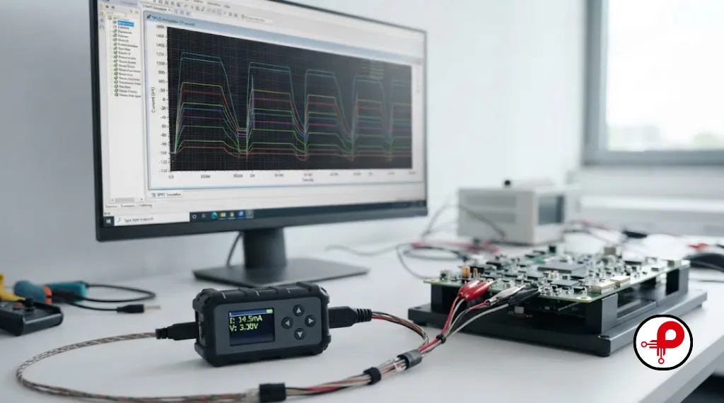
You cannot optimize what you haven’t measured. Low power circuit design lives or dies on validation.
Simulation and Estimation
SPICE-level simulation catches leakage and switching behavior at the transistor level; RTL power estimation tools catch architectural issues (excessive toggling, missing clock gates) before layout. Both matter: RTL tools are fast but approximate, and SPICE is accurate but too slow to run on every design iteration.
Bench Measurement
This is where theory meets reality. A current-sense amplifier feeding an oscilloscope or a dedicated power profiler (like a Power Profiler Kit or a precision source-measure unit) lets you see actual current draw across sleep/wake transitions, often revealing spikes or leakage that never show up in a datasheet-based estimate. I flag any unexplained current step on a profiler trace before signing off on a board, because it almost always points to a missed sleep configuration or a pull-up left floating.
Design for Test and Manufacturing
Power-related failures are notoriously hard to catch in standard functional test. Building current-draw checkpoints into your PCB testing and inspection process, measuring quiescent current at each major sleep state during production test, catches assembly defects (solder bridges, wrong component values) that a purely functional pass/fail test would miss entirely. This connects to broader PCB testing practices that should be built into your production line from day one, not bolted on after a field failure.
[Visual suggestion: an oscilloscope capture showing current draw across an MCU’s active-to-sleep transition, annotated with each power state.]
Common Mistakes in Low Power Circuit Design
These show up repeatedly across client projects, regardless of team experience level:
Low-Power Design Pitfalls & Mistakes
Trusting Typical Datasheet Current Values
Quiescent current can vary 2-5x across temperature and input voltage range; always check the full operating envelope, not just the headline number.
Leaving Unused GPIOs Floating
Floating inputs can draw unexpected current through internal pull structures and cause erratic switching that wastes power continuously.
Ignoring Inrush and Wake-up Transients
A device that averages 10µA but spikes to 40mA for 5ms on every wake event can still drain a coin cell faster than expected if wake events are frequent.
Over-provisioning Clock Speed “For Margin”
Running a processor faster than the workload requires wastes power quadratically for no functional benefit; right-size the clock to the actual task.
Skipping Firmware-Level Power Auditing
A perfectly designed low-power board can still be defeated by a busy-wait loop or a peripheral left enabled after use; firmware discipline is part of low power circuit design, not separate from it.
Underestimating Antenna and RF Mismatch Losses
A poorly matched antenna forces a radio to transmit longer or at higher power to achieve the same range, which directly hits battery life.
Choosing Components in Isolation from the Full BOM
The lowest-power MCU paired with an inefficient regulator can lose to a “less efficient” MCU paired with a well-matched power supply; always evaluate power at the system level, not the component level.
Best Practices Checklist
Use this before every design review on a power-sensitive project:
Low-Power Hardware & Firmware Design Checklist
Verification Steps
Frequently Asked Questions
1. What is low power circuit design?
↑2. What is the difference between dynamic and static power?
↓3. What causes leakage power in CMOS transistors?
↓4. Which is better for low power: clock gating or power gating?
↓5. What is duty cycling in low power design?
↓6. Why does my battery-powered device drain faster than expected?
↓7. How do I choose a low power microcontroller?
↓8. What’s the biggest mistake teams make in low power design?
↓Key Takeaways and Conclusion
Low power circuit design isn’t a single technique; it’s a discipline that spans transistor-level choices, IC architecture, PCB layout, and firmware, and it has to be budgeted from day one rather than patched in after prototypes fail battery-life targets.
Key takeaways:
- Dynamic power scales with voltage squared, making voltage scaling and duty cycling the highest-leverage techniques for most board-level designs.
- Leakage power matters more than ever on modern process nodes, especially for idle-heavy, battery-powered applications.
- Power gating, clock gating, and multi-Vt design each target different parts of the power budget; most real designs combine several techniques rather than relying on one.
- Board-level decisions, component selection, PCB layout, regulator topology, can undo silicon-level efficiency gains if treated as an afterthought.
- Bench validation of actual current draw, not datasheet estimates, is the only reliable way to confirm a low power design meets its targets.
If you’re starting a new battery-powered, IoT, or medical product and want power budgeted correctly from the first schematic rather than debugged after prototypes miss their targets, our team works through this exact process daily across product development, embedded systems development, and rapid prototyping engagements. Reach out to talk through your power budget before your next board spin; it’s far cheaper to solve on paper than in a field return.
Related resources: PCB Design vs. PCB Layout | Electronic Component Selection Guidelines | Medical Device Development | Industrial Product Design Engineering | ESP32 Selection Guide | How to Certify an Electronic Product | Why Hardware Startups Fail
Further technical reading: TI Low-Power Development Guide (MSPM0 Power Optimization) | TI Ultra-Low-Power Design with MSP430 | Analog Devices: Power Optimization Techniques for Low Power Signal Chains | Microchip AN1416: Low-Power Design Guide | Microchip AN1267: eXtreme Low-Power PIC Microcontrollers | Arm Cortex-M Low-Power Mode Fundamentals