










Component failures rarely happen because a part was defective out of the box. In my eight years designing and validating electronic hardware, the majority of field failures I have investigated trace back to one root cause: a component was pushed too close to its rated limits under real world stress. That is exactly the problem electronic component derating guidelines exist to solve.
This guide walks through what electronic component derating guidelines actually mean at the physics level, which derating standards govern component selection across industries, how to calculate a derating factor for every major component family, and how to build these electronic component derating guidelines into your design and verification process from schematic capture through PCB testing and inspection. It is written for engineers who need practical numbers, a working derating chart, and checklists, not just theory.
What Are Electronic Component Derating Guidelines
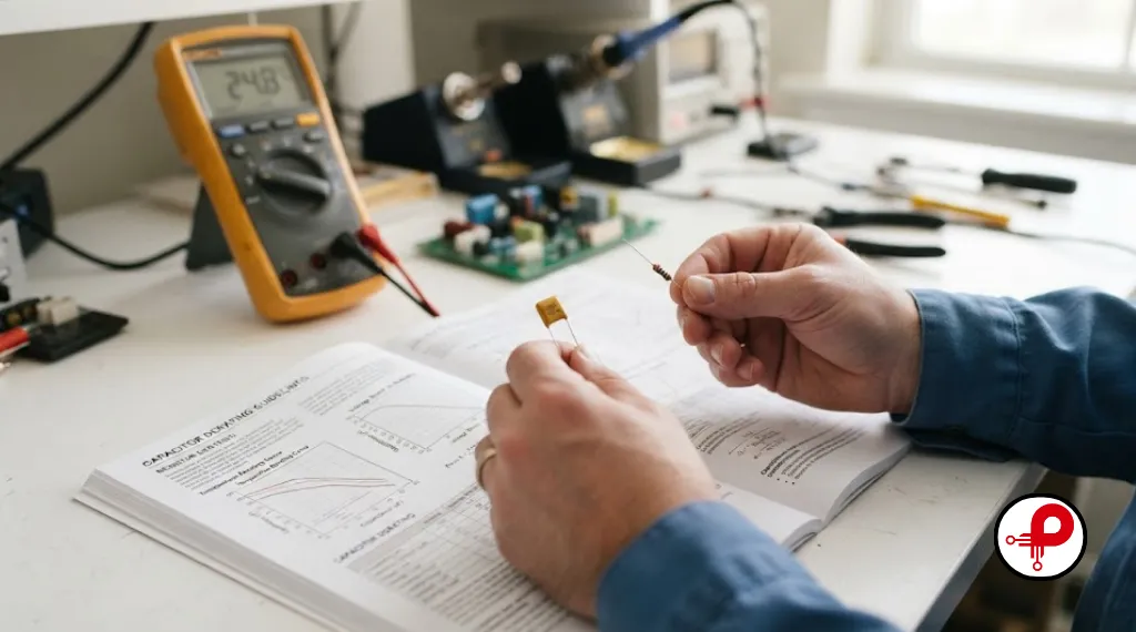
Electronic component derating guidelines define how far below a manufacturer’s absolute maximum rating a part should be operated for voltage, current, power, and temperature, so that actual operating stress leaves a safety margin against the component’s true physical limits. A resistor rated for 0.25 W is not run at 0.25 W in a well designed circuit; power derating typically limits it to somewhere between 0.125 W and 0.175 W depending on ambient temperature and the reliability target set by your internal electronic component derating guidelines.
The core idea behind every derating factor is simple: every stress placed on a component, whether electrical, thermal, or mechanical, accelerates the physical and chemical mechanisms that eventually cause it to fail. Reducing that stress slows the aging process and pushes the failure point further into the future. Component reliability references describe this practice as reducing thermal, electrical, and mechanical stresses on parts to levels below their manufacturer specified absolute maximum rating in order to improve long term reliability.
Featured snippet answer: Electronic component derating guidelines define how much lower than its rated voltage, current, power, or temperature a part should be operated, typically expressed as a derating factor or percentage (for example, 70% of rated voltage), in order to reduce stress induced failure mechanisms and extend service life.
The Physics Behind Voltage Derating and Current Derating
Electronic component reliability depends on controlling thermal, electrical, and mechanical stresses that accelerate failure. Arrhenius-based models show how temperature affects semiconductor life, while voltage and current stresses can accelerate dielectric degradation and electromigration. Effective derating therefore limits components below their maximum ratings, reducing heat generation and material stress while improving long-term reliability, stability, and service life in demanding applications.
Thermal Stress & Reliability Mechanics
Thermal Stress
Higher junction temperatures accelerate physical degradation, making thermal management essential for maintaining semiconductor reliability and extending operating life.
Arrhenius Model
The Arrhenius relationship explains how increasing temperature accelerates failure mechanisms and reduces expected component operating lifetime significantly.
Voltage Derating
Operating capacitors below maximum voltage reduces dielectric stress, slowing insulation degradation and improving long-term component reliability.
Current Derating
Limiting current reduces junction heating and electromigration, helping MOSFETs and other power components maintain reliable performance.
Recommended Ratings
Effective derating keeps components within recommended operating conditions rather than approaching absolute maximum ratings during normal operation.
Why Electronic Component Derating Guidelines Matter for Reliability and MTBF
Skipping electronic component derating guidelines does not usually cause an immediate failure. The board powers on, passes functional test, and ships. The real cost shows up months or years later as field returns, warranty claims, and in some industries, safety incidents. A properly derated design directly improves Mean Time Between Failures (MTBF), reduces the frequency of thermally induced intermittent faults, and gives your product margin against manufacturing tolerances, component aging, and worst-case analysis conditions found in the field.
This is why formal electronic component derating guidelines are not optional in aerospace, defense, medical, automotive, and industrial control programs. They are written into contractual specifications, and derating analysis is one of the first things a customer’s quality team will ask about during a design review. Even in consumer and IoT products where formal derating standards are not mandated, ignoring component stress derating is one of the most common reasons hardware startups run into expensive field failures after launch, a mistake I cover in more depth in why hardware startups fail.
Major Electronic Component Derating Standards Compared
Several organizations publish formal electronic component derating standards, and the right one to follow depends on your industry and reliability requirements. Below is a comparison of the electronic component derating standards I reference most often in practice.
Most commercial and industrial companies do not adopt a military standard wholesale. Instead, based on my experience across multiple product lines, engineering teams typically build internal electronic component derating guidelines that borrow the numeric derating factor tables from EEE INST 002 or MIL STD 975 and adapt them to the reliability level the product actually needs. That approach gives you defensible, standards based electronic component derating guidelines without over engineering a consumer product to space flight tolerances.
For teams that want the original source material, the NASA EEE INST 002 derating instructions and the NASA Preferred Reliability Practices guide on EEE parts derating are freely available and remain the most widely referenced derating curves and tables in the industry.
Electronic Component Derating Guidelines by Component Type
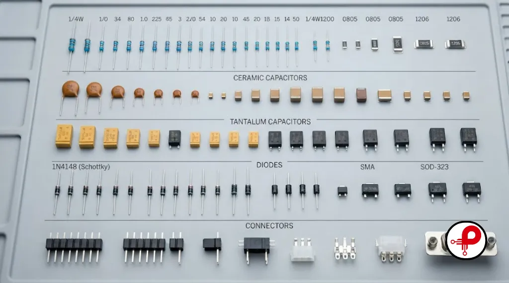
Generic percentages are a starting point, not a substitute for reading the actual datasheet derating curve or recommended operating conditions table. Every component family has its own dominant failure mechanism, so the electronic component derating guidelines below target that mechanism specifically rather than applying one flat derating factor across the whole bill of materials.
Resistor Power Derating Guidelines
Resistor power dissipation must be derated as ambient temperature rises. Manufacturers publish a power derating curve that typically holds full absolute maximum rating up to around 70°C ambient, then linearly reduces allowable power to zero at the component’s maximum rated temperature, often 155°C for film resistors. A commonly used industrial electronic component derating guideline limits resistors to no more than 50% of rated power at the design’s expected worst case ambient temperature, with additional margin for resistors mounted close together or in poorly ventilated enclosures.
Practical formula for linear power derating:
P(derated) = P(rated) x (1 minus ((T ambient minus T1) / (T max minus T1)))
Where T1 is the temperature at which power derating begins (commonly 70°C) and T max is the zero power temperature specified in the recommended operating conditions section of the datasheet.
Electronic Component Derating Chart for Capacitors
Capacitor voltage derating factors vary significantly by dielectric type because each has a different dominant wear out mechanism. The following electronic component derating chart summarizes the values I use most often during schematic review.
Aluminum electrolytic capacitors deserve special attention because their electrolyte dries out over time, and that process accelerates sharply with temperature and ripple current. A widely used rule of thumb is that electrolytic capacitor life roughly doubles for every 10°C reduction in operating temperature, which is why power supply designers pay close attention to keeping electrolytics away from hot components during PCB layout.
Semiconductor Current Derating: Diodes, Transistors, and ICs
Semiconductor derating centers on junction temperature and current density, and it is the area where electronic component derating current calculations matter most. Common industry starting points include limiting continuous current to 70 to 75% of the datasheet absolute maximum rating, keeping junction temperature at least 20 to 25°C below the absolute maximum rating, and derating reverse voltage on diodes to around 70% of the rated breakdown voltage to guard against transient overvoltage events.
For high complexity microcircuits and COTS (commercial off the shelf) devices used in demanding environments, current derating gets more nuanced. Industry reliability studies have shown that indiscriminately derating advanced microcircuits without understanding the internal architecture can sometimes create more risk than it removes, because internal timing margins and process node sensitivities do not always scale the way passive components do. This is one reason semiconductor manufacturers like Texas Instruments and Analog Devices publish device specific application notes rather than relying purely on generic electronic component derating guidelines.
Connector and Relay Current Derating
Connectors are commonly derated on both voltage and current. A frequently cited electronic component derating guideline limits continuous current to no more than 80% of the connector’s rated maximum, with additional derating for contact resistance increase over the product’s service life. For high voltage connectors, the derating factor is often calculated against the dielectric withstand voltage (DWV) rating rather than the working voltage rating alone, since DWV testing establishes the true breakdown margin.
Inductors, Transformers, and Magnetics
Magnetic components are typically derated on both current derating, to avoid core saturation and excessive winding temperature rise, and on operating temperature relative to the insulation class of the winding material. A common approach limits continuous current to 80% of the rated saturation current and keeps hot spot winding temperature at least 20°C below the insulation class limit.
How to Calculate an Electronic Component Derating Factor
The general derating calculation follows the same pattern regardless of component type, and it is the core of any credible electronic component derating guidelines document:
Identify Absolute Maximum Rating
Identify the manufacturer’s absolute maximum rating for the stress parameter (voltage, current, power, or temperature).
Select Derating Factor
Select the appropriate derating factor from your governing electronic component derating standards or internal guideline, based on component type and required reliability level.
Calculate Allowed Operating Stress
Multiply the rated value by the derating factor to get the maximum allowed operating stress, which becomes your new recommended operating conditions target.
Compare Worst-Case Circuit Stress
Compare your actual worst-case analysis circuit stress, calculated at worst case tolerances, against that derated limit.
Mitigate Over-Stress Conditions
If actual stress exceeds the derated limit, select a higher rated part, redesign the circuit, or improve thermal derating through better cooling.
Worked example of an electronic component derating calculation: A tantalum capacitor is rated for 35 VDC. Using a 60% voltage derating factor for wet slug tantalum in a design with an ambient temperature under 70°C, the maximum allowed operating voltage becomes 35 x 0.6, which equals 21 VDC. If the circuit’s worst case applied voltage, including supply tolerance and transient spikes, is 24 VDC, that part selection fails the electronic component derating calculation and a higher voltage rated capacitor is required.
This is exactly the kind of worst-case analysis that should happen during schematic review, before the design moves into electronic hardware design sign off and into layout.
Thermal Derating and Its Link to Component Reliability
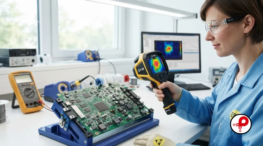
Thermal derating and component reliability are inseparable. Every derating chart assumes a specific ambient or case temperature, and if your enclosure, airflow, or PCB copper design cannot hold components at that assumed temperature, your derating margin evaporates even if the electrical stress numbers look fine on paper.
Key thermal factors that directly affect how much derating margin a design actually has in practice include enclosure ventilation and orientation, copper pour area and thermal via placement under power components, component spacing to avoid localized hot spots, and heatsink or thermal interface material selection for high dissipation parts. Thermal imaging during prototype bring up is one of the fastest ways to catch a component that looks fine in simulation but is running hotter than expected on the actual board, which is a standard part of validation during PCB testing and inspection.
Electronic Component Derating Guidelines During PCB Design and Layout

Derating decisions made at the schematic level can be undermined by layout choices, so electronic component derating guidelines need to carry through into the physical design. A few layout specific considerations worth building into your design rules include keeping high power resistors and regulators away from temperature sensitive electrolytic capacitors, following the circuit board design rules for trace width versus current carrying capacity so copper traces themselves are current derated correctly, using adequate copper weight and via stitching for high current paths, and separating PCB design from PCB layout responsibilities carefully so thermal derating and voltage derating requirements from the schematic phase are not lost when the board is physically routed.
RF sections deserve a specific mention here. Components near an antenna feed, for example in a 2.4 GHz PCB antenna design, often see higher transient voltage stress from ESD and near field coupling, so derating margins in that area are typically tightened rather than loosened.
Electronic Component Derating Guidelines for Specific Application Environments
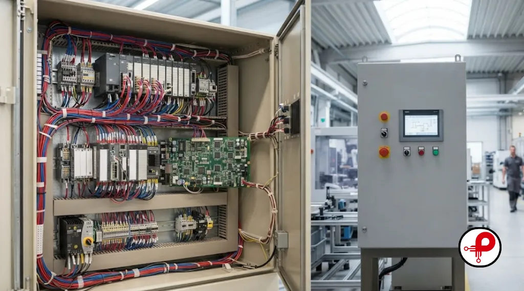
Different industries apply different derating philosophies depending on consequence of failure, expected service life, and access for repair.
Aerospace and Defense
These programs typically follow MIL STD 975, EEE INST 002, or ECSS Q ST 30 11C directly, with formal electronic component derating guidelines documented and reviewed as a contractual deliverable. Margins are aggressive because field repair is impossible or extremely costly.
Medical Devices
Medical electronics balance patient safety with practical manufacturability. Electronic component derating guidelines here are closely tied to the regulatory certification process, and a documented derating and worst-case analysis is often expected as part of design history file evidence during medical device development.
Industrial Control
Industrial equipment, including PLCs, motor drives, and I/O modules, targets long service life, typically 10 to 20 years, in uncontrolled thermal environments. Derating factors here are often similar to military guidelines but applied more selectively to control cost, focusing the tightest margins on power supply and switching components that see the highest voltage derating and current derating stress.
Consumer, IoT, and Wearable Products
Consumer grade products generally do not follow formal military derating standards, but skipping component stress derating analysis entirely is a common source of early field failures, particularly in battery powered and wearable designs where thermal derating is constrained by small enclosures. When I work on wearable technology development or general IoT development projects, I still apply lightweight electronic component derating guidelines internally, typically 20 to 30% margin on voltage and current for critical components, even without a formal standard driving it. Battery management ICs, charging circuits, and wireless modules such as those covered in the ESP32 selection guide benefit especially from conservative thermal derating given how compact these enclosures tend to be.
Industrial and Heavy Equipment Product Design
Larger industrial and heavy equipment platforms, the kind covered under industrial product design engineering, often combine multiple stress factors at once, vibration, wide temperature swings, and long duty cycles, which is why component stress derating analysis on these programs typically extends beyond electrical stress into mechanical and connector level derating as well.
Common Derating Mistakes Engineers Make
Even experienced teams fall into a handful of recurring traps when applying electronic component derating guidelines.
Common Derating Pitfalls & Mistakes
Ignoring Operating Temperature
Using room temperature ratings without adjusting for actual worst case ambient or enclosure temperature.
Ignoring Ripple Current Derating
Ignoring ripple current derating on electrolytic capacitors, focusing only on voltage derating.
Generic Derating Factors
Applying a single generic derating factor across all component families instead of using part specific electronic component derating standards.
Forgetting PCB Traces
Forgetting that PCB copper traces and vias need current derating too, not just discrete components.
Skipping Worst-Case Analysis
Skipping worst-case analysis, so nominal circuit values look fine but corner case combinations exceed the absolute maximum rating.
Excessive IC Derating
Over derating advanced digital ICs without understanding internal timing margins, which can introduce new component reliability risks rather than removing them.
Missing Late-Stage Re-Verifications
Not re-verifying electronic component derating guidelines after a component substitution or second source part is introduced late in production.
Treating Derating as One-Time
Treating derating as a one time schematic exercise instead of validating derating curves with real thermal and electrical measurements during prototype testing.
Practical Electronic Component Derating Guidelines Checklist
Use this checklist during design review and before releasing a board for fabrication.
Component Derating & Thermal Verification Checklist
Verification Steps
Real World Case Study
On a battery powered industrial sensor project I worked on, early prototypes used a compact buck converter with a 100 microfarad ceramic output capacitor rated for 16 VDC in a nominal 12 VDC rail. On paper the design looked fine against our internal electronic component derating guidelines, since the nominal operating voltage sat comfortably under the rated maximum. During thermal validation, however, load transients combined with input supply tolerance pushed instantaneous voltage spikes above 14.5 VDC, which put the capacitor at roughly 90% of its rated voltage rather than the 60% voltage derating target from our internal guideline. Combined with the DC bias derating that ceramic capacitors experience, actual effective capacitance under those conditions had dropped enough to create marginal transient response.
The fix was straightforward once identified: switch to a 25 VDC rated capacitor of the same case size and dielectric, which restored the voltage derating margin to target and eliminated the transient behavior entirely in the next build. The lesson that stuck with me from that project is that derating checks done only against nominal supply voltage will miss real world transient stress, which is exactly why worst-case analysis, not just nominal analysis, has to be part of any electronic component derating guidelines process.
Best Practices From Production Experience
Build electronic component derating guidelines checks into your schematic review checklist rather than treating them as a separate audit late in the program. Use a spreadsheet or dedicated derating analysis tool to track every critical component’s absolute maximum rating, applied derating factor, and calculated margin in one place, since manual tracking across hundreds of parts is where mistakes happen. Base your internal electronic component derating guidelines on an established standard such as EEE INST 002 rather than inventing derating factors from scratch, even for commercial products, because it gives you defensible numbers during customer audits. Always validate derating assumptions with actual thermal measurement on early prototypes rather than relying solely on simulation. Revisit voltage derating and current derating whenever a component is second sourced, since electrical and thermal characteristics can vary meaningfully between manufacturers even for parts with identical part numbers on paper.
Quick Decision Guide
Use this simple decision path when you are unsure how aggressively to apply electronic component derating guidelines to a given part.
If the product is aerospace, defense, or space flight, follow MIL STD 975, EEE INST 002, or ECSS Q ST 30 11C directly and document formal worst-case analysis.
If the product is medical or safety critical, apply internal electronic component derating guidelines based on EEE INST 002 derating factor tables and document them as part of your design history file and product development records.
If the product is industrial with a 10 plus year service life, apply moderate derating, generally 60 to 80% of rated values depending on component type, focused heavily on power stage components.
If the product is consumer or IoT with a shorter expected service life, apply lightweight derating, generally 20 to 30% margin on critical power and RF components, and prioritize thermal derating validation on the first prototype.