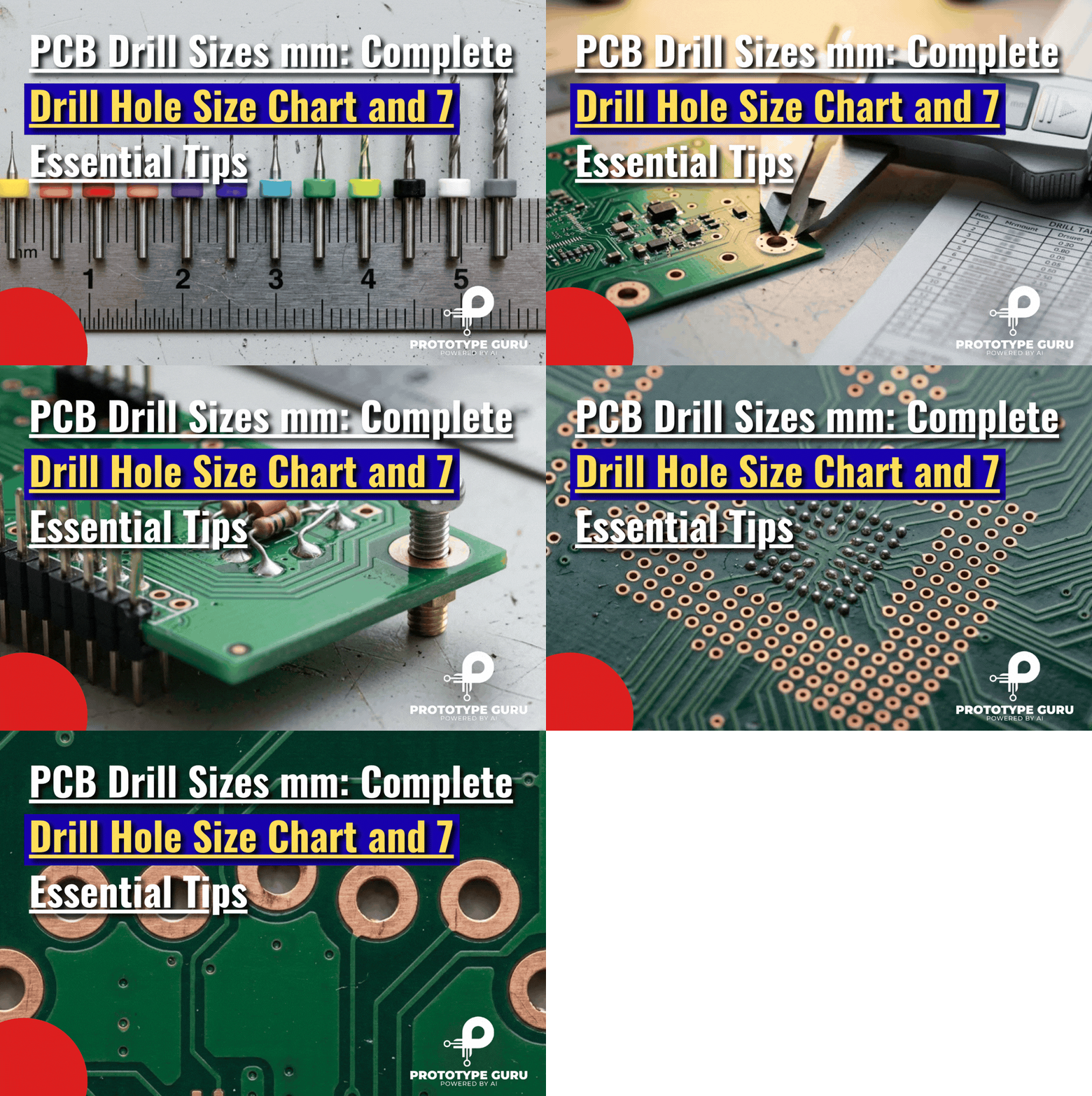









Choosing the right PCB drill sizes mm values is important for a board that can be manufactured and assembled reliably. Hole diameter affects component fit, copper around the hole, and fabrication cost.
No single list of PCB drill sizes mm suits every manufacturer or application. Use this chart as a starting point, then confirm finished size, plating status, and tolerance with the component datasheet and fabricator.
Quick answer: common PCB drill sizes mm that designers may consider include 0.20 mm, 0.25 mm, 0.30 mm, 0.40 mm, 0.50 mm, 0.60 mm, 0.80 mm, and 1.00 mm, with larger sizes used for some leads and mounting features. The right choice depends on the actual pin or hardware, the role of the hole, the board stackup, and the manufacturer’s process.
1. PCB Drill Sizes mm: Quick Reference Chart
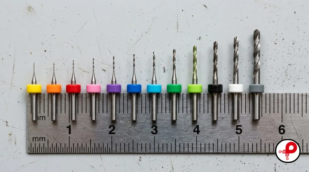
A PCB drill chart of PCB drill sizes mm lists the nominal diameters used for vias, component leads, mounting hardware, tooling holes, and other openings. Designs usually specify dimensions in millimetres, although imperial dimensions and mils also appear in older drawings and some supplier tables. One mil is 0.001 inch, or 0.0254 mm.
The table below gives common PCB drill sizes mm values, often called common PCB drill sizes or typical PCB drill sizes, with their approximate mil equivalents. These are practical CAD reference values, not a guarantee that every factory has a production drill for each diameter. Manufacturers can use fixed tool increments or convert submitted dimensions according to their own production rules.
| Nominal diameter in mm | Approximate diameter in mils | Typical design context |
|---|---|---|
| 0.20 | 7.9 | Small via where supported |
| 0.25 | 9.8 | Small via or compact plated hole |
| 0.30 | 11.8 | Common via design starting point |
| 0.35 | 13.8 | Small plated hole or via |
| 0.40 | 15.7 | Via or small component hole |
| 0.45 | 17.7 | Small lead hole or larger via |
| 0.50 | 19.7 | Small connector lead, depending on pin dimensions |
| 0.60 | 23.6 | Component hole or via |
| 0.70 | 27.6 | Component lead hole when specified |
| 0.80 | 31.5 | Starting point for some through hole leads |
| 0.90 | 35.4 | Larger lead or header hole |
| 1.00 | 39.4 | Larger pin or lead |
| 1.20 | 47.2 | Connector or mechanical feature |
| 1.50 | 59.1 | Larger component or mechanical hole |
| 2.00 | 78.7 | Hardware or clearance feature |
| 2.50 | 98.4 | Mounting clearance feature |
| 3.00 | 118.1 | Larger mechanical clearance feature |
These PCB drill sizes mm are rounded conversions, not universal recommendations. A 0.30 mm via may suit one stackup but be too small or too expensive for another. For production, review the supplier’s capability table. JLCPCB publishes its own drill and hole tolerances, while E Tek’s drill chart separates finished plated hole dimensions from tool sizes. These tables use supplier specific rules.
To convert PCB drill sizes mm to mils, multiply by 39.3701. To convert mils to millimetres, multiply by 0.0254. Confirm units in CAD output and fabrication drawings before approval.
2. How to Read a PCB Drill Chart Correctly
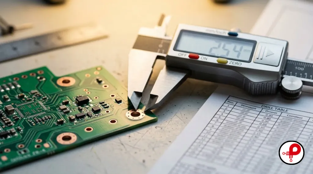
A chart of PCB drill sizes mm is only useful when you understand what its dimensions describe. A number in a CAD footprint may represent the intended finished opening or, in some workflows, the physical drill tool. These are related but not always equal, so clarify the meaning before sending data to a manufacturer.
Finished hole size and drill tool diameter
The finished hole size is the usable opening in the delivered board. The drill tool diameter is the size of the tool used at the drilling stage. In a plated hole, copper is deposited on the wall, reducing the open diameter. The tool therefore often needs to be larger than the finished hole you require.
Eurocircuits’ drilled hole guidelines describe one production rule: its tool size for a plated through hole is normally 0.10 mm larger than the finished size, while its nonplated tool size matches the finished dimension. This is the Eurocircuits process, not a rule for every factory. Follow the specific supplier’s instructions.
In most ordinary design workflows, specify the finished opening needed by the component or mechanical function and let the fabricator apply its own compensation. Do not add a plating allowance yourself unless the supplier explicitly requests tool diameters. Adding compensation twice can make a finished hole too large.
Plated holes and nonplated holes
A plated through hole, or PTH, has a conductive barrel and can connect copper layers or accept a soldered lead. A nonplated through hole, or NPTH, has no conductive barrel and is commonly used for mechanical clearance, alignment, or tooling. A mounting hole may be plated when it needs a ground or other electrical connection.
Identify the intended hole type clearly in the CAD data and fabrication notes. The KiCad PCB Editor documentation distinguishes through hole pads with plated holes from NPTH mechanical pads without an electrical connection.
Holes, slots, and cutouts are not interchangeable
A drilled hole, plated slot, nonplated slot, and board cutout can have different manufacturing limits. Slot dimensions and tolerances depend on the manufacturer. Do not imitate a slot with overlapping holes unless the fabricator approves it.
Check the units, finished or tool size convention, plating status, and published tolerance before using any chart of PCB drill hole sizes.
3. Standard PCB Drill Sizes mm by Application
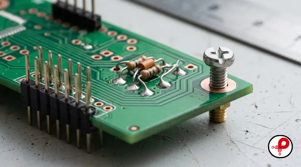
There is no universal set of standard PCB drill sizes mm for each component type. Start with the actual pin, lead, screw, or mechanical feature, then account for fit, manufacturing variation, pad geometry, and supplier rules. A generic chart cannot replace a component drawing.
Component leads and connectors
Check the component datasheet for a recommended finished PCB hole diameter. If no value is supplied, use the maximum lead or pin dimension as the starting point, then determine the insertion clearance needed for your assembly process. For a square or rectangular pin, consider the diagonal dimension because the corners span more space than the side measurement suggests.
This matters for headers, terminal blocks, transformer pins, and connectors. Press fit pins need a controlled interference fit, so follow the connector maker’s hole and tolerance requirements. For broader assembly context, see PrototypeGuru’s SMT vs Through Hole guide.
PCB hole sizes for mounting holes and screws
A screw’s nominal diameter is not automatically the right PCB clearance hole size. A clearance hole is usually larger than the screw, and its size depends on whether the fit should be close, normal, or loose, along with enclosure alignment and assembly tolerance.
A finished nonplated hole around 3.2 mm to 3.4 mm can be a preliminary choice for some M3 clearance applications, but it is not a universal rule. Check the screw or standoff drawing, intended fit, and manufacturer’s tolerance. Apply the same method to M2, M2.5, or M4 hardware instead of choosing from the thread label alone.
For a grounded mounting hole, decide whether it should be plated. For an isolated hole, maintain the required copper and solder mask clearances.
Wire leads, tooling holes, and test access
Wire gauge alone cannot determine a hole size because stripped wire, ferrules, and terminal pins vary. For terminal blocks, use the pin dimensions in the component drawing. Tooling holes need reliable position as well as diameter, while test access needs enough space for the probe. PrototypeGuru’s PCB Design for Testability guide offers related test access guidance.
Verify unusual PCB drill sizes mm with the fabricator before releasing the board.
4. PCB Drill Sizes mm for Vias and Small Features
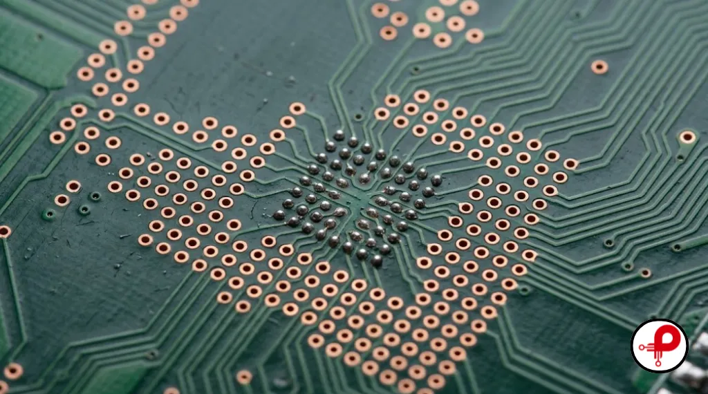
Vias connect copper layers, so the PCB drill sizes mm you choose for them affect routing density, pad size, annular ring, current capacity, plating reliability, and cost. A smaller via can save space, but it is not automatically the best choice. It may require a more specialised process or be unavailable for a particular board thickness or layer stack.
Standard PCB via drill sizes
When planning standard PCB via drill sizes, designers may evaluate finished via holes such as 0.20 mm, 0.25 mm, 0.30 mm, or 0.40 mm, depending on the design. These are planning examples rather than guaranteed standards. A manufacturer may support smaller holes only under certain conditions or recommend a larger size for cost and yield.
For instance, JLCPCB’s published capability information lists a 0.15 mm hole with a 0.25 mm via diameter for some multilayer services, and describes narrower conditions for smaller microvia options. Review its latest capability specifications before selecting one of these values. For further planning, see PrototypeGuru’s PCB Via Design Guide.
A via includes a hole and surrounding copper land. The pad must preserve the required annular ring after drill variation and layer registration, so a smaller drill may not reduce the full footprint as much as expected.
Board thickness and aspect ratio
Aspect ratio describes the relationship between board thickness and the relevant drilled diameter. A thick board with a small through hole creates a higher aspect ratio, which can make uniform barrel plating more difficult. The exact limit depends on the supplier’s manufacturing process and board construction, so there is no single safe ratio to assume for every design.
For a very small hole or thick board, ask the fabricator to confirm the combination. The PrototypeGuru HDI PCB Design Guide provides more context for dense interconnects.
Mechanical drilling and laser microvias
Mechanical drills produce many component holes and vias. Laser drilling can form small microvias for high density interconnect designs, but microvias may need particular layer relationships, capture pads, filling, or sequential lamination.
Use the smallest PCB drill sizes mm only when needed, then validate the hole, pad, aspect ratio, stackup, and process together. KYOCERA Precision Tools publishes real PCB drill bit sizes as a manufacturing reference, which shows how standard PCB drill bit sizes are made in practice.
5. PCB Drill Sizes mm: Drill Tool Size Versus Finished Hole Size
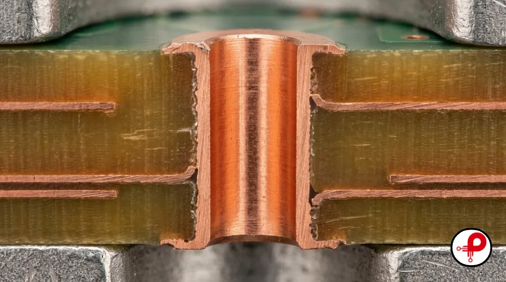
When reading PCB drill sizes mm, confusing the drill tool size with the finished hole size can cause component fit problems, incorrect clearances, and manufacturing delays. The safest approach is to specify the functional opening you need, verify how your CAD software exports drill dimensions, and confirm how the selected fabricator interprets that data.
Why plating changes a hole
A plated hole is drilled through the laminate, then copper is deposited on the hole wall to connect copper layers. That copper takes up space inside the opening, so the finished diameter is smaller than the original drill diameter. A nonplated hole does not receive the same conductive barrel, so its finished size is more directly related to the tool, though manufacturing variation still applies.
Eurocircuits documents a 0.10 mm drill oversize for its plated through holes. PCBWay publishes its own manufacturing tolerances, including finished hole ranges that demonstrate why tool size and finished size must be distinguished. These values belong to their respective manufacturers and should not be combined into a universal formula.
Worked example
Suppose a connector datasheet calls for a 0.80 mm finished plated hole. Under a process that uses a 0.10 mm oversize, the fabricator may choose a 0.90 mm drill tool. In the usual workflow, you specify the required finished 0.80 mm dimension and let the manufacturer’s CAM system apply compensation.
This arithmetic is illustrative only, and it shows why PCB drill sizes mm in your CAD file should normally describe the finished hole. If the manufacturer defines submitted files differently or uses another compensation amount, its documented procedure takes priority. Do not change a 0.80 mm CAD hole to 0.90 mm without confirming that tool diameter is actually required.
Drill files and design output
EDA tools commonly generate Excellon drill data alongside Gerber or other fabrication outputs. Before ordering, check units, diameters, counts, and the PTH or NPTH classification. State whether dimensions are finished sizes unless the supplier requires another convention. If separate plated and nonplated files are needed, label them clearly and ask the fabricator to review uncertain data. PrototypeGuru’s PCB Manufacturing and Assembly Process guide explains the wider workflow.
6. PCB Drill Size Tolerance, Plating and Annular Rings
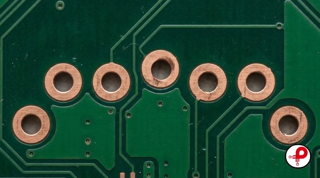
PCB drill size tolerance is the allowed variation around a specified dimension, and it applies to all PCB drill sizes mm in your design. Hole size tolerance describes how large or small the opening may be, while positional tolerance describes how far the hole centre may move from its designed location. A hole can meet its diameter tolerance and still create a problem if it is misplaced relative to a narrow copper pad.
Why the numbers differ by supplier
Manufacturers publish different tolerances for plated holes, nonplated holes, slots, press fit holes, and hole diameter ranges. JLCPCB, PCBWay, and Eurocircuits each publish their own capability values. Associate every number with its supplier and conditions.
For connector fits, press fit contacts, or alignment pins, state the required tolerance and ask the fabricator to confirm capability. Tighter tolerances may require a specialised service. See Eurocircuits’ finished hole tolerance guidance and Altium’s tips for specifying PCB hole tolerances.
Annular ring and copper clearance
The annular ring is the copper left around a hole, supporting electrical continuity and reliability on plated pads. A large or misplaced hole may leave too little copper on one side.
For a circular pad, the nominal radial ring is half the pad diameter minus half the hole diameter. A 1.40 mm pad around a 0.80 mm finished hole has a nominal ring of 0.30 mm before manufacturing allowances. This is only a geometric estimate. Apply the relevant design and supplier rules to judge acceptability.
Altium’s PCB drill sizing guide explains why drill diameter and pad dimensions should be designed together. Also check drill to copper clearance, plus spacing to traces, planes, neighbouring holes, and board edges. When checking the worst case clearance, account for the production tool diameter and specified position tolerance where the fabricator’s rules require it. For broader spacing guidance, use PrototypeGuru’s PCB Layout Best Practices guide.
7. How to Choose PCB Drill Sizes mm and Avoid DFM Problems
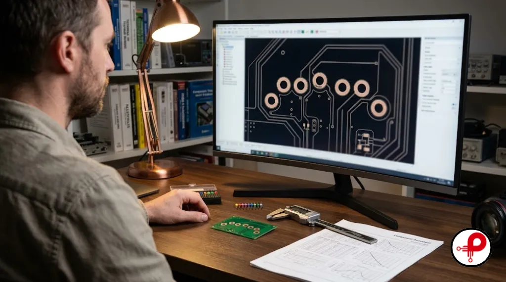
Choosing PCB drill sizes mm starts by identifying the hole’s function. A signal via, component lead, screw, tooling point, press fit contact, and routed slot have different requirements. Use the relevant part dimensions, then check the manufacturer’s capabilities.
A practical selection workflow
Identify the function
Check the part drawing
Choose the finished diameter
Check the pad and nearby copper
Validate the stackup
Read the capability table
Review the manufacturing output
Common mistakes to catch before ordering
Do not use a screw’s nominal diameter as its clearance hole without checking the intended fit. Do not calculate square pin clearance from the pin side alone. Do not apply plating compensation twice. Avoid using the smallest via just because it is listed as available, and do not assume every supplier supports the same tolerance.
Other problems include insufficient copper, wrong plating classification, mismatched units, and overlapping holes used to imitate a slot. For mounting features, confirm electrical intent and copper clearance. For board separation, use an appropriate panelization method and check the design against the fabricator’s panel requirements.
Review the part datasheet, CAD rules, drill file, and manufacturer capabilities together before you freeze your PCB drill sizes mm. Request DFM review for holes critical to assembly.
8. Seven Essential Tips for Choosing PCB Drill Sizes mm
Use these seven checks on your PCB drill sizes mm before releasing a board for fabrication. They do not replace manufacturer rules, but they create a repeatable final review.
Define the hole’s purpose
Separate electrical vias, component lead holes, mounting holes, tooling holes, test access, and slots. Their function affects plating, tolerance, pad shape, and minimum size.
Use real component dimensions
Check the latest component drawing and recommended PCB hole. Consider the maximum lead size and the diagonal of a square pin. Ask the manufacturer when the specified fit is unclear.
Keep finished size separate from tool size
Confirm whether your CAD output represents finished holes or physical drill tools. Do not add plating compensation unless the fabricator explicitly requires it.
Design the pad with the hole
Check the annular ring after accounting for hole variation and position tolerance. Rerun your design rule checks whenever the hole or pad changes.
Use smaller vias only when needed
Small vias save routing room, but may raise cost and process requirements. Validate the stackup, aspect ratio, pad size, and supplier capabilities before selecting them.
Treat mechanical fit separately
Screws, standoffs, tooling pins, and press fit contacts need different tolerances. A screw’s nominal diameter is not its clearance hole size, and a press fit hole should follow the contact maker’s specification.
Make the fabrication data clear
Ensure hole counts, sizes, tolerances, and plating requirements are clearly defined in your fabrication drawings and drill schedules to prevent misunderstandings.
Confirm units, diameters, hole counts, and plating status. State special tolerances and requirements in the drawing, then verify the output files before approval.
The best PCB drill sizes mm are the ones that meet the component or mechanical requirement, preserves adequate copper, and matches the chosen fabrication process. A PCB drill sizes mm chart is a useful starting point, but accurate documentation and manufacturer review make the design production ready.
Frequently Asked Questions
1. What are standard PCB drill sizes in mm?
↑Available production sizes depend on the supplier and on whether the dimension means finished hole or drill tool.
2. What is the difference between drill size and finished hole size?
↓Copper plating reduces the opening in plated holes, so the tool may be larger than the required finished dimension. Confirm the selected manufacturer’s convention.
3. What is a typical PCB via drill size?
↓Confirm pad diameter, annular ring, aspect ratio, and manufacturing availability with your fabricator.
4. What hole size should I use for an M3 screw on a PCB?
↓Around 3.2 mm to 3.4 mm can be a preliminary example for some applications, but the correct choice depends on the required fit, hardware drawing, and hole tolerance.
5. How much larger should a PCB hole be than a component lead?
↓For square pins, consider the diagonal dimension.
6. What is PCB drill size tolerance?
↓Plated and nonplated holes can have different tolerances, and each supplier publishes its own limits. Position tolerance is different because it describes the allowed movement of the hole centre.
7. What is the difference between PTH and NPTH?
↓The feature should be identified clearly because plating changes the manufacturing process and can affect the finished diameter.