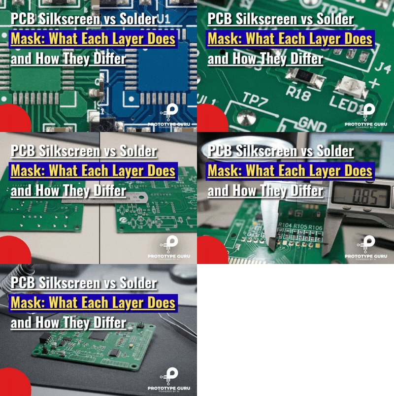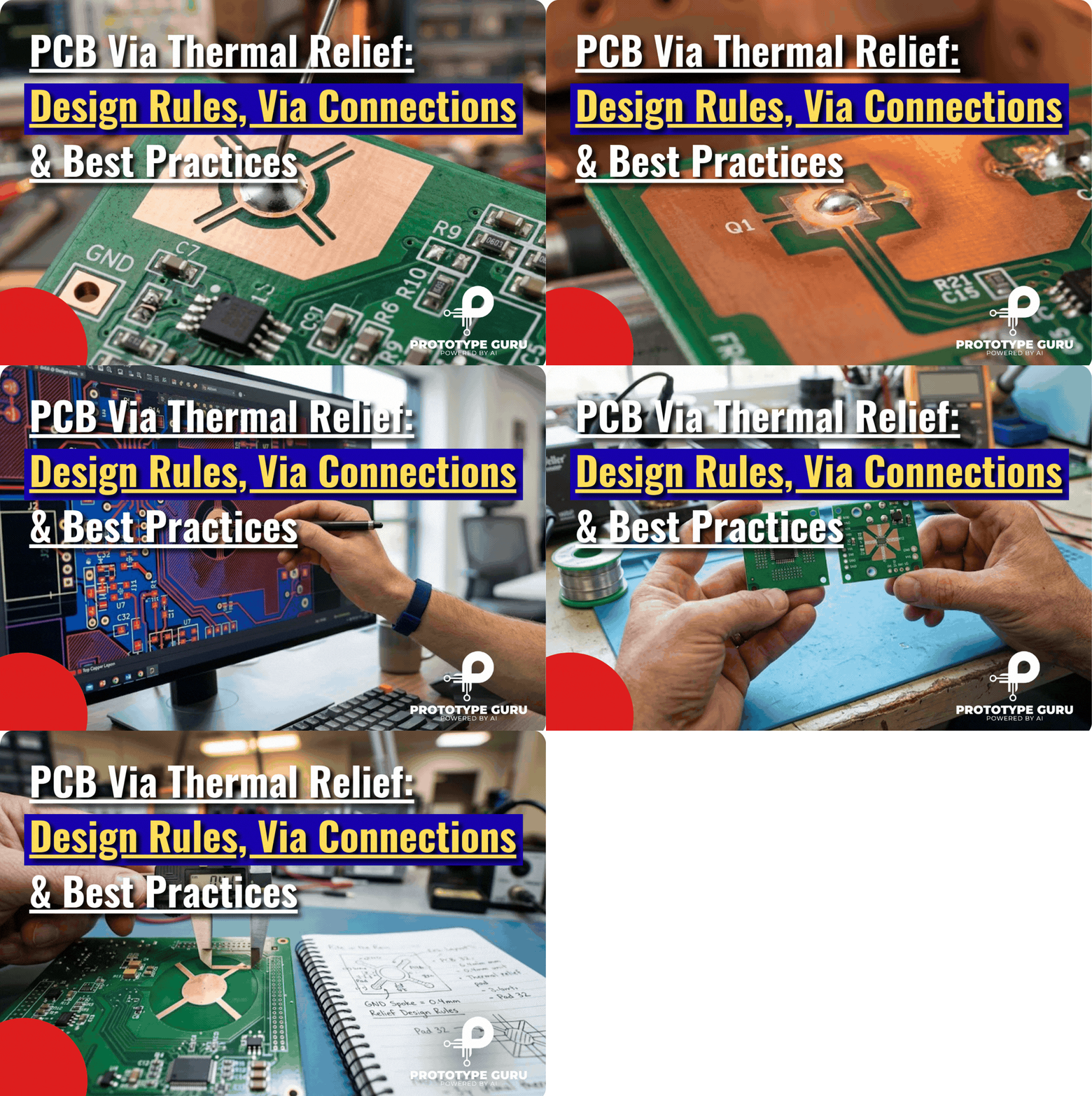











The difference between pcb silkscreen vs solder mask comes down to purpose. Solder mask is the thin polymer coating that covers the copper traces, protects them from oxidation and stops solder from bridging between pads. Silkscreen is the printed ink legend on top of that coating, which carries reference designators, polarity marks, logos and test labels so people can assemble, test and repair the board. Solder mask protects the board. Silkscreen helps humans read it.
If you only remember one line, remember this one: mask is functional and electrical, silkscreen is informational and mechanical. A board can run without silkscreen. It will be hard to build and debug, but it works. A board without solder mask is a very different story, and we will get to why.
I have spent more than eight years reviewing layouts before they go to a fabrication house, and these two layers cause a surprising share of the questions that come back from the fab. Most of them are not exotic. They come from people treating both layers as decoration. This guide explains what each layer really does, how they interact, the numbers that matter, and a checklist you can run before you export your Gerber files.
What Is Solder Mask on a PCB?

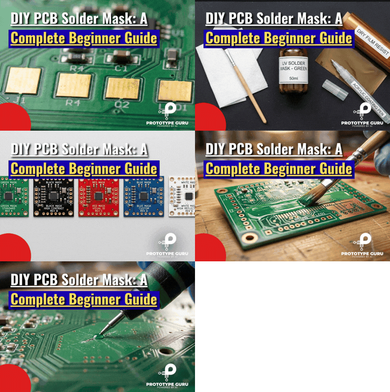
Solder mask, also called solder resist or soldermask, is a thin protective layer applied over the outer copper layers of a printed circuit board. Its colour is the first thing most people notice about a board, and green is still the most common, but the colour is the least interesting part of the story. The Wikipedia entry on solder mask gives a good neutral definition if you want a quick reference.
What solder mask actually does
- It stops solder from flowing where it should not. During reflow or wave soldering, molten solder wants to wet any exposed copper. The mask confines solder to the pads you meant to expose.
- It prevents solder bridges on fine pitch parts. The thin strip of mask between two pads is called a solder dam, and it is what keeps neighbouring pins from shorting.
- It protects copper from oxidation, moisture, dust and light handling damage.
- It adds a layer of insulation between traces and anything that touches the board, which helps with creepage in real products.
- It makes inspection easier, because pads stand out clearly against the coated surface.
How it is applied
Most boards today use liquid photoimageable solder mask, usually shortened to LPI. The fab coats the board, exposes it through a film or by laser direct imaging, develops away the areas that should stay open, then cures the rest. Dry film mask exists and is used for certain high reliability or thick copper jobs, but for ordinary prototype and production boards LPI is the standard.
The mask is thin. Figures quoted by fabricators typically land around 0.5 to 1.5 mil, roughly 0.013 to 0.038 mm. GlobalWellPCBA notes this range in its comparison, and I have seen very similar numbers in fab capability sheets. That thickness is enough for protection but nowhere near enough to count as a serious dielectric for high voltage work, so do not design creepage around mask alone.
Mask openings and pads
Wherever the layout needs solder, the mask has an opening. For surface mount pads, the opening is normally slightly larger than the copper pad. That extra margin is the mask expansion. Too small and the mask can creep onto the pad edge, which hurts solder wetting. Too large and you lose the dam between pins. Typical guidance, including the FastTurnPCBs process guide, puts expansion in the range of 3 to 5 mil per side and a minimum dam of about 4 mil, although the exact limits depend on the fab and the mask colour.
Mask colour matters in practice. Green is the best supported and usually the cheapest. Black and white masks can need wider dams because the pigments behave differently during imaging. If you are designing a very fine pitch part, check the fab’s rules for your chosen colour before committing.
What Is Silkscreen on a PCB?

Silkscreen, also called legend or nomenclature, is the printed text and symbols on the surface of the board. The name comes from the original screen printing process, though most modern boards use direct legend printing, which is closer to inkjet.
What belongs on silkscreen
Reference Designators
Unique labels such as R12, C4, and U3 assigned to every component on the schematic and layout to streamline assembly and BOM matching.
Polarity & Pin Markers
Cathode bars, plus signs, shaded regions, and pin 1 indicators (dots, notches, or bevels) for diodes, LEDs, capacitors, and ICs.
Connector Labels & Signals
Clear pinout indicators and signal names on external headers and connectors to prevent wiring mistakes during prototyping.
Board Identification
Official project name, hardware revision number, and manufacturing date codes to track design iterations accurately.
Test Point Labels
Clearly designated test pad markings positioned adjacent to probing points with sufficient clearance for manufacturing checks.
Logos & Regulatory Marks
Company branding, open-source hardware symbols, and necessary compliance marks placed on empty top or bottom board zones.
Assembly Alignment Outlines
Body dimension outlines matching components to aid manual placement, automated optical inspection, and clearance verification.
Two-Column Grid Layout
A structured, side-by-side card grid optimized for clean visual hierarchy, readability, and modern dashboard presentation.
Silkscreen is non conductive epoxy or similar ink, cured after printing. It is not meant to be an electrical or protective layer. It is there for people and sometimes for machine vision during assembly.
How silkscreen is printed
There are three methods you are likely to encounter. Traditional screen printing pushes ink through a mesh stencil and gives acceptable results for larger text. Liquid photoimageable legend is imaged like the mask and can produce finer detail. Direct legend printing uses an inkjet style head that prints from the digital file directly, and it is the method behind the smallest text most fabs now offer. The PCBMay comparison mentions text as small as roughly 0.1 mm with laser direct imaging style processes, though I would never design to that limit on a board someone else has to read.
Colour and contrast
White ink on a green mask is the classic combination because it reads clearly under almost any lighting. On a black mask, white is still the best choice. On a white mask, use black ink. Yellow ink on a dark mask also works but is less common. The rule I follow is simple: the legend should be readable at arm’s length under ordinary workshop light, because that is where it will actually be read.
PCB Silkscreen vs Solder Mask: Side by Side Comparison
This table pulls the main differences into one place. It is the part most readers want when they search for this comparison, so I kept it compact.
| Feature | Solder Mask | Silkscreen |
|---|---|---|
| Main purpose | Protect copper and control solder flow | Label components and guide assembly and repair |
| Typical material | Polymer, usually LPI epoxy based | Epoxy or similar legend ink |
| Typical thickness | About 0.5 to 1.5 mil | Very thin ink layer, fab dependent |
| Covers copper? | Yes, except in openings for pads and vias you leave exposed | Sits on top of mask or bare laminate, never meant for pads |
| Electrical role | Insulating coating, solder dam | None, do not rely on it as insulation |
| Common colours | Green, black, white, blue, red, yellow | White, black, sometimes yellow |
| When applied | After copper etching, before the legend | After the mask has been cured |
| What happens if omitted | Bridging, corrosion, poor yield | Hard to assemble, test and debug, but board still works |
| Typical failure when done wrong | Mask on pads, missing dams, pinholes | Unreadable text, ink on pads, reversed polarity marks |
| Who benefits most | The board and the solder joint | The technician and the engineer |
A quick note on the order of operations. The mask goes on first and the legend goes on afterward. Depending on the fab, the surface finish such as HASL or ENIG may be applied before or after the legend, which is one reason ink and exposed metal rules differ slightly between factories. Always read your fab’s process notes rather than assuming.
How the Two Layers Work Together

The two layers share a surface, so they interact in ways that catch people out.
Silkscreen sits on top of the mask
On a normal board, the legend is printed on the cured mask, which is why white text looks crisp against green. It adheres well there. It also adheres to bare laminate where there is no copper.
Silkscreen over exposed copper gets removed
This one surprises beginners. If your legend overlaps a pad, an exposed copper area, or a tinned or gold plated region, many fabs will clip or delete that ink automatically, because ink on a solderable surface ruins the joint. JLCPCB’s character specification page states plainly that characters on exposed copper areas are removed. The result is text with missing pieces, which looks like a bug in your design when it is really the fab protecting yield.
Printing silkscreen directly on bare copper
It is technically possible but not routine. Forum answers, such as this PCBGOGO question and answer, report that fabs either decline it or strip the layer before production unless they have agreed to it. If your design genuinely needs ink on copper, talk to the fab before you order.
Mask openings control where silkscreen can safely go
Think of the mask openings as the keep out zones for your legend. Anywhere the mask is open, the silkscreen should be absent. A good CAD tool lets you set a silk to mask clearance rule, and I recommend using it. It saves you from discovering the problem when the clipped text comes back on the finished boards.
Vias and mask
Vias add another layer of decisions. A tented via is covered by mask, which protects it and keeps solder out. An untented via has an opening and exposes the barrel. For vias near fine pitch pads, tenting reduces solder wicking. For vias you want to probe, leave them open. Whatever you choose, keep legend text off them. Ink in a via opening can trap contaminants and confuse inspection.
Interaction with assembly and testing
Pick and place machines usually rely on fiducials, pads and component outlines, not on the legend. Still, ink that drifts onto a fiducial can reduce its contrast and cause alignment trouble. In test and rework, the legend is your map. If you want a solid overview of how markings feed into inspection and test access, our guide on PCB testing and inspection covers what technicians really look for on a finished board.
Design Numbers That Matter
Every fab has its own capabilities, so treat these as common starting points, not universal law. Check your chosen manufacturer’s capability page every time you switch factories, and use their DRC profile if one is available for your CAD tool.
| Parameter | Common minimum | Safer target | Source note |
|---|---|---|---|
| Silkscreen character height | 1.0 mm (40 mil) | 1.0 mm or larger | JLCPCB specifications |
| Silkscreen stroke width | 0.15 mm (6 mil) | 0.18 to 0.20 mm | JLCPCB and other fab guides |
| Silkscreen clearance from pads | 0.15 mm | 0.25 mm or more | JLCPCB |
| Gap between characters | Above 0.15 mm | 0.2 mm or more | JLCPCB |
| High precision text height | 0.8 mm (32 mil) | Avoid unless essential | JLCPCB |
| Solder mask expansion | 3 mil per side | 3 to 5 mil | FastTurnPCBs |
| Minimum solder dam | About 4 mil | Wider where possible | FastTurnPCBs, fab dependent |
| Mask thickness | 0.5 to 1.5 mil | Set by fab | GlobalWellPCBA |
A few engineering notes on reading that table.
Do not design to the absolute minimum
The minimum is what the fab can hold on a good day with a well tuned line. Designing at the limit means your yield drops the moment ink thickness or registration drifts slightly. If space allows, go larger. Text at 1.2 mm height with a 0.2 mm stroke is far more readable than text that technically passes at 1.0 mm and 0.15 mm.
Registration is the hidden variable
Both layers are applied after the copper is etched, and each application has its own alignment tolerance. A mask opening can shift a little relative to the pad, and ink can shift relative to the mask. That is why generous silk to pad clearance and mask expansion matter more than a perfect looking CAD view.
Dams shrink on dense parts
On a fine pitch QFN or BGA, the mask dam between pads can become so narrow that the fab cannot hold it. Some fabs will remove the dam and open the mask as one window for the whole row of pins, which raises bridging risk. If your design depends on dams, check the capability for your pitch and mask colour early, not at the end of layout. For a wider view of layout rules that affect these choices, see our PCB layout best practices article.
Standards worth knowing
IPC publishes the standards that fabs and assemblers reference for land patterns, acceptability and solder mask requirements. The land pattern guidance in IPC 7351, which Sierra Circuits’ explanation of IPC 7351 covers well, is the reason your footprint pad sizes and mask openings look the way they do in most libraries.
Real Failures to Watch For

These are patterns that come up again and again when boards are reviewed. They are described as scenarios because the details differ from board to board, but the causes are consistent.
Reversed polarity from an unclear mark
A polarity dot placed inside the component body outline disappears once the part is placed. The technician cannot see it, so the diode or LED goes on backward. The fix is to put polarity marks outside the body, in a spot that stays visible after assembly. Better still, mark pin one on the board edge of the footprint and also mirror it in the assembly drawing.
Tombstoning from ink on pads
If silkscreen stretches across a small chip resistor pad, the ink can lift one side of the part during reflow, because the pad wets unevenly. The part stands on one end, like a tombstone. This is common on 0402 and 0201 parts. Keep legend away from every pad, and run a silk to pad check in your CAD tool.
Solder bridges from missing dams
A designer enlarges the mask opening to be safe, forgetting that it also removes the mask strip between two close pins. During reflow, solder joins the pins. The fix is to keep the dam, reduce the expansion on that footprint, or choose a part with more generous pitch if the fab cannot hold the dam.
Mask creeping onto pads
If the expansion is zero or negative, mask can cover a sliver of the pad edge, and the joint ends up smaller than the stencil expected. This is more subtle than a bridge. The board may pass visual inspection and still show weak or inconsistent joints. Using a standard expansion, as in the table above, avoids it.
Text clipped by the fab
Legend that overlaps a mask opening or exposed copper gets clipped, and the reference designator becomes unreadable. Run a DRC check for silk over openings before you export. I treat this one as non negotiable.
Unreadable labels from tiny text
Text below the fab’s practical limit prints as a smear. Reference designators on dense boards are the usual victims. If a board is too crowded for readable labels, move designators to a separate assembly drawing instead of shrinking the text on the board.
Poor contrast on coloured masks
White ink on a yellow or light blue mask can be almost invisible. Test your colour combination on a small run before committing to a large order. A mask colour that looks great in a render is not always the one that photographs well in a repair manual.
Silkscreen ink assumed to insulate
Occasionally someone tries to rely on legend ink or mask as insulation between exposed conductors in a high voltage design. Neither is reliable for that job. Use proper clearance and creepage distances based on the applicable standard and the working voltage.
Quick Decision Guide

Use this guide to decide what each layer should do on your next board.
Do I need solder mask?
- Almost always yes. Skip it only on very simple hobby boards you will hand solder, and even then the bare copper corrodes faster and bridges more easily.
- Choose LPI for ordinary boards. Consider dry film only if your fab recommends it for thick copper or special reliability work.
- Pick green unless there is a real reason to choose another colour. It is the best supported and tends to give the tightest dams.
Do I need silkscreen?
- On any board that someone will assemble, test or repair by hand, yes.
- On a tiny production board with an assembly drawing and machine placement, you can often reduce the legend to a board name, revision and polarity marks.
- On a space constrained board, drop reference designators first and keep polarity marks and test point labels.
What should always stay on the legend?
- Polarity and pin one markers
- Board name and revision
- Test point labels
- Connector orientation or pin labels
- Safety or regulatory marks required for your product
What can you drop if space is tight?
- Part values, since the BOM carries them
- Decorative graphics
- Redundant labels that repeat what the schematic already shows
If your product is heading toward a formal design process, our overview of the electronic product design workflow shows where these decisions fit among schematic, layout, fabrication and test.
Pre Gerber Checklist
Run this list before you send files to the fab. It takes about ten minutes and prevents most of the questions that bounce back.
For general layout discipline that helps with this check, our guide on circuit board design rules explains how to set up rules in your CAD tool so these errors are caught automatically. If you are still deciding where design ends and layout begins, the difference is explained in PCB design vs PCB layout.