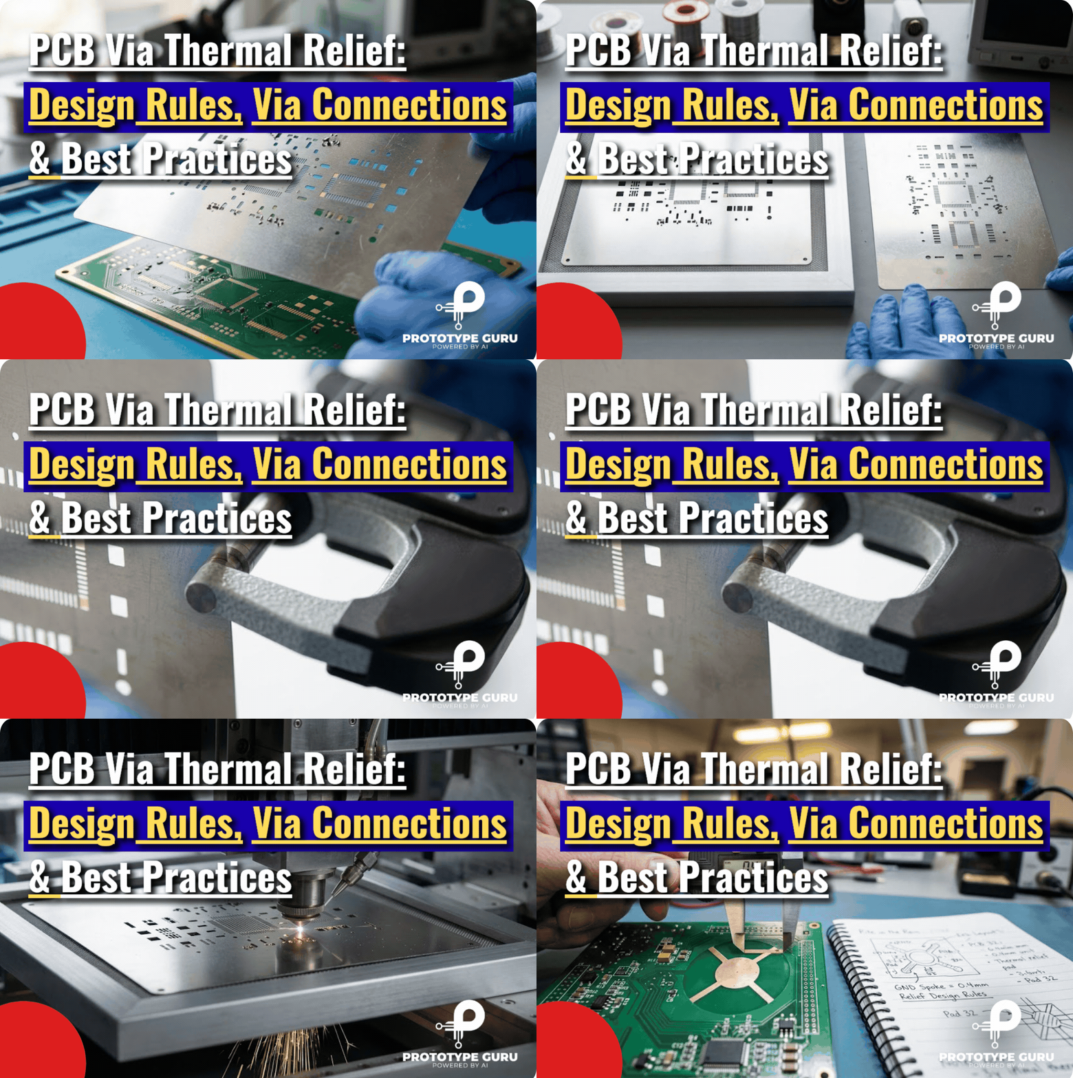




A PCB stencil is a thin metal sheet, usually stainless steel, with openings cut exactly where solder paste must go on a printed circuit board. You lay it on the board, spread solder paste across it with a squeegee, and lift it away. Paste stays only on the surface mount pads, ready for components and reflow.
That is why it is often called a solder paste stencil or SMT stencil. It is not a craft stencil for drawing circuit art, and it is not the same thing as solder mask.
Most PCB stencils are between 0.10 mm and 0.15 mm thick. The right thickness depends on your smallest parts, and the right openings depend on a few simple ratios. This guide explains both, along with stencil types, how stencils are made, how to use one, what goes wrong, what they cost, and what to send when you order.
What Is a PCB Stencil?
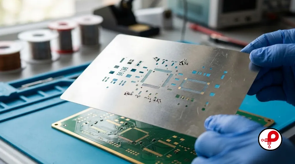
A PCB stencil is a tool for putting the right amount of solder paste in the right place. Each opening, called an aperture, matches a pad in your design. When paste is pushed through the aperture, a small, even deposit lands on the pad below.
The volume of that deposit matters more than most beginners expect. Too little paste gives weak or open joints. Too much paste causes bridges between pins and solder balls around parts. A good stencil controls both the position and the volume of every deposit on the board.
The Purpose of a PCB Stencil
A stencil for PCB assembly has three main jobs:
Accuracy
Consistency
Speed
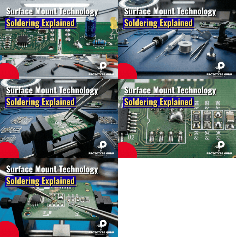
This is why stencil printing is the first step in almost every surface mount technology line, before pick and place and reflow. Our SMT soldering guide explains what happens next.
PCB Stencil vs Solder Mask
Beginners often confuse these two. Solder mask is a permanent coating on the board, usually green, that covers copper you do not want to solder. A PCB stencil is a separate, reusable tool that only touches the board during paste printing.
You need both: the solder mask keeps solder off traces, and the stencil puts paste on pads. If you want to learn about the coating itself, read our guide to DIY PCB solder mask.
Do You Need a Stencil for Solder Paste?
Not always. For a single prototype with a few large parts, you can apply paste by hand from a syringe. Once you have fine pitch ICs, many small passives, or more than a couple of boards, a PCB stencil saves time and gives far better results.
For QFN, BGA and 0402 or smaller parts, a stencil is close to essential. Hand dispensing simply cannot control such small paste volumes reliably.
PCB Stencil Types and Materials
PCB stencils come in several formats. The right one depends on how many boards you build and how you print them.
| Type | What it is | Best for |
|---|---|---|
| Frameless (prototype) stencil | A flat foil with no frame, aligned by hand or with a simple jig | Prototypes and small batches |
| Framed stencil | Foil glued into a rigid aluminium frame under tension | Production printers and large volumes |
| Tensioned frame system stencil | A foil that clips into a reusable tensioning frame | Medium volume, saving storage space |
| Step stencil | A foil with thinner or thicker areas in one sheet | Boards mixing fine pitch and large parts |
| Electroformed stencil | Nickel foil built up by plating, with very smooth walls | Ultra fine pitch and the best paste release |
Frameless vs Framed Stencils
A frameless PCB stencil is the usual choice for prototypes. It is cheaper, easy to store, and works with a manual printing jig or even taped down on a bench.
A framed stencil holds the foil flat and tight, which a production printer needs for repeatable alignment and clean release. It costs more and takes more storage space, but it is the standard for volume assembly.
PCB Stencil Material
Most stencils are laser cut from stainless steel, which is strong, durable and affordable. Electroformed stencils are made from nickel and have extremely smooth aperture walls, which helps paste release from tiny openings.
Many suppliers also offer finishing options:
- Electropolishing: smooths the aperture walls so paste releases more cleanly.
- Nano coating: a thin coating that repels flux and paste, reducing smearing and cleaning.
For most prototypes, a plain laser cut stainless steel stencil is perfectly adequate.
PCB Stencil Thickness: How to Choose
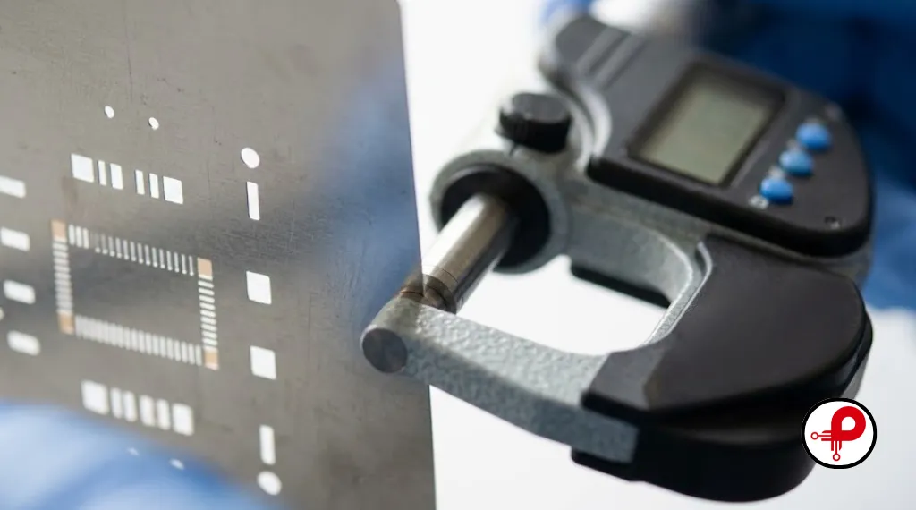
PCB stencil thickness sets how much paste each pad receives. Thicker foil gives more paste, while thinner foil gives less paste but releases better from small openings.
The rule is simple: choose the thickness for the finest pitch part on your board. The table below comes from the guidance published by Bittele Electronics, which bases its thickness rules on the IPC 7525 stencil design guideline.
| Component | Pitch | Suggested stencil thickness |
|---|---|---|
| Chip 0201 | n/a | 0.12 mm |
| Chip 0402 | n/a | 0.10 mm |
| QFP or QFN | 0.65 mm | 0.15 mm |
| QFP or QFN | 0.50 mm | 0.13 mm |
| QFP or QFN | 0.40 mm | 0.12 mm |
| QFP or QFN | 0.30 mm | 0.10 mm |
| BGA | 1.25 to 1.27 mm | 0.15 mm |
| BGA | 1.00 mm | 0.13 mm |
| BGA | 0.5 to 0.8 mm | 0.12 mm |
How Thick Is a PCB Stencil?
Most PCB stencils are 0.10 mm, 0.12 mm, 0.13 mm or 0.15 mm thick (roughly 4 to 6 mils). A thickness of 0.12 mm is a common all round choice for boards with typical modern parts.
When to Use a Step Stencil
Sometimes one thickness cannot satisfy every part. A fine pitch QFN may need 0.10 mm, while a large connector or power inductor needs more paste from 0.15 mm. A step stencil solves this by making part of the foil thinner or thicker.
Step stencils cost more, so try adjusting aperture sizes first. Only move to a step stencil when aperture changes cannot balance the paste volumes.
Do not confuse PCB stencil thickness with board thickness. If you need the board itself, see our PCB thickness guide.
PCB Stencil Design: Apertures, Area Ratio and Paste Layer
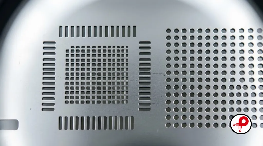
PCB stencil design is mostly aperture design. The openings start from your pads, then get adjusted so paste releases cleanly and the right volume lands on each pad.
Aspect Ratio and Area Ratio (IPC 7525)
Two ratios predict whether paste will release from an aperture. Bittele summarizes the IPC 7525 values like this:
| Rule | Formula | Minimum value |
|---|---|---|
| Aspect ratio | Aperture width ÷ stencil thickness (W ÷ T) | 1.5 |
| Area ratio | (L × W) ÷ (2 × (L + W) × T) | 0.66 |
In plain words, the area ratio compares the area of the opening with the area of its walls. If the walls are too large compared with the opening, paste sticks to the walls instead of dropping onto the pad.
Worked Example: A QFN Pad at Two Thicknesses
Take a QFN pad aperture of 0.25 mm by 0.60 mm and check it at two common thicknesses:
| PCB stencil thickness | Area ratio | Aspect ratio | Result |
|---|---|---|---|
| 0.12 mm | 0.735 | 2.08 | Passes both rules |
| 0.15 mm | 0.588 | 1.67 | Fails the area ratio rule |
At 0.15 mm the area ratio drops below 0.66, so paste would not release reliably. Moving to a 0.12 mm PCB stencil fixes it without changing the pad. This is exactly why thickness should follow your finest pitch part.
Fine Pitch Parts: QFN, BGA, QFP and 0201
Small parts need extra care in stencil design:
- QFN thermal pads: do not open the large centre pad as one big aperture. Split it into a grid of smaller openings, often called windowpaning, so the part does not float on too much paste.
- BGA: use round or square apertures close to the pad size, and check the area ratio for the smallest balls.
- Fine pitch QFP: slightly narrow the apertures to reduce bridging between pins.
- 0201 and 0402 chips: small apertures quickly fail the area ratio, so thinner foil helps.
For more detail on aperture shapes, JLCPCB’s aperture design guide and AtlasPCB’s stencil design article are useful references. Good pad design also matters, so review our PCB layout best practices and DFM and DFA guidelines.
Exporting the Gerber Paste Layer
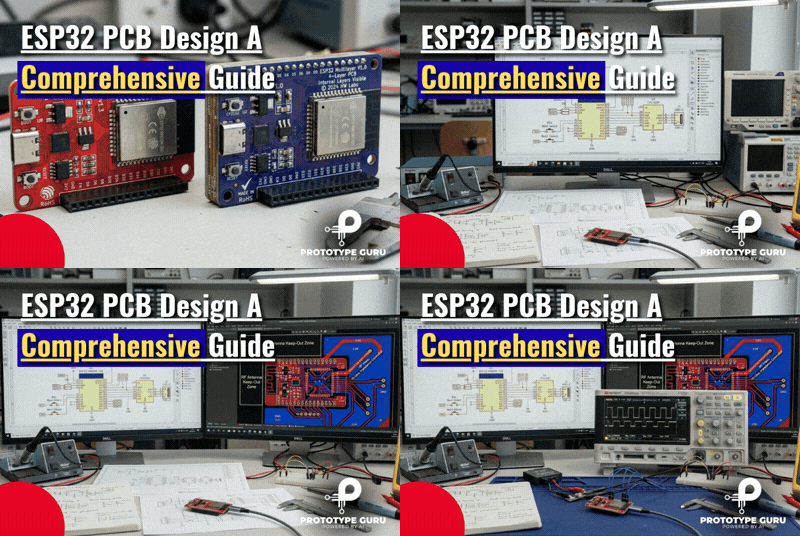
Your PCB stencil is cut from the paste layer in your design files, not from the copper layer. In KiCad this is the F.Paste and B.Paste layer. In other tools it may be called top paste or the solder paste layer.
Before ordering, open the paste Gerber in a viewer and check that:
- Every SMD pad has an aperture.
- Through hole pads have no paste unless you plan pin in paste soldering.
- Large thermal pads are split into smaller openings.
- Fiducials and board outline are present for alignment.
The KiCad PCB Editor documentation explains how paste margins and layers work.
Match the Solder Paste to the Apertures
Paste choice and aperture size work together. Solder paste is graded by the size of its metal powder, using type numbers defined in the J STD 005 standard. Type 3 paste has larger particles and suits most general boards, while Type 4 and Type 5 pastes use finer powder for very small apertures.
A common rule of thumb is that the narrowest aperture should be at least about five particles wide. If your smallest openings are very narrow, a finer paste type can improve release just as much as a thinner foil. Ask your assembler which paste they use before you finalize very small apertures.
Aperture Size Compared With the Pad
Apertures are not always the same size as the pads. For most chip resistors and capacitors, a slightly reduced aperture helps prevent solder balls. For fine pitch leads, narrowing the aperture a little reduces bridging. For large pads and connectors, apertures are sometimes enlarged or split to get the right paste volume.
Many fabricators apply their own standard reductions automatically. That is convenient, but it can clash with changes you already made in your design tool. Decide who adjusts the apertures, you or the supplier, and say so clearly when you order.
How a PCB Stencil Is Made
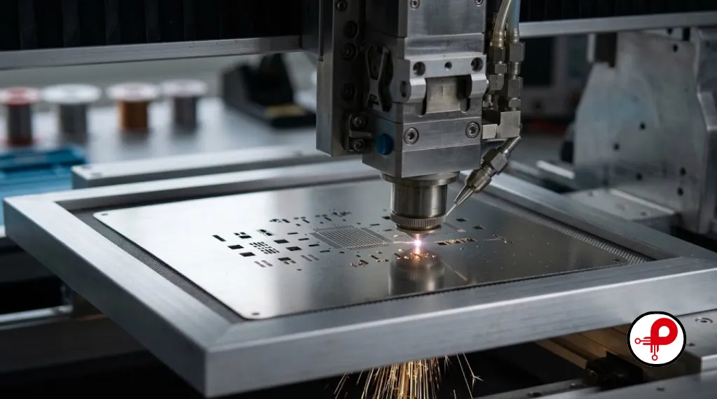
Knowing how a stencil is made helps you choose the right type and price level.
Laser Cut Stencils
Most PCB stencils today are laser cut. A precise laser cuts each aperture directly from a stainless steel sheet using your paste Gerber. It is fast, accurate and suitable for almost all prototypes and production boards.
After cutting, the stencil is cleaned and may be electropolished or nano coated to improve paste release.
Electroformed Stencils
Electroformed stencils are made by plating nickel onto a patterned base, building the foil up layer by layer. The aperture walls end up very smooth, which helps with ultra fine pitch parts. They cost more and take longer, so they are usually reserved for demanding production work.
How to Make a Stencil for a PCB Yourself
Hobbyists sometimes make DIY stencils from polyimide film or thin plastic with a laser cutter or a desktop vinyl cutter. These can work for larger pads and a few boards.
For fine pitch parts, DIY stencils struggle with accuracy and paste release. Low cost laser cut stainless steel stencils from online fabricators are usually the better choice. Our overview of the PCB manufacturing and assembly process shows where the stencil fits in the full build.
How to Use a Stencil for PCB Assembly
PCB stencil printing is simple once your setup is stable. These steps work for a manual jig and translate directly to a production printer:
Fix the board
Hold the PCB flat in a jig or between spare boards of the same thickness, so it cannot move.
Align the stencil
Line up the apertures with the pads using the fiducial marks or the pads themselves. Tape a frameless stencil on one edge like a hinge so you can lift and check it.
Add paste
Place a bead of solder paste along one side, above the apertures. Use paste at room temperature and stir it gently first.
Print in one stroke
Pull a metal squeegee across at about 45 to 60 degrees with firm, even pressure. One smooth pass is better than several passes.
Lift straight up
Separate the stencil from the board slowly and evenly to avoid smearing.
Inspect the paste
Check that every pad has a clean, even deposit before placing parts.
Clean the stencil
Wipe the underside regularly during a batch and clean it fully when you finish, so dried paste does not block small apertures.
For hand assembly tips after printing, our guide to soldering tips for beginners covers the basics.
Manual Jig or Stencil Printer?
A manual setup is fine for prototypes and small batches. A simple jig holds the board, and a hinged frameless stencil gives repeatable alignment for a few dozen boards.
A semi automatic or automatic stencil printer controls squeegee speed, pressure and separation, and often uses a camera to align with fiducials. It costs far more, but it gives consistent results for larger runs. If you plan to outsource assembly, your assembler will already have a printer, and you only need to supply a framed stencil or let them order one.
Cleaning, Storage and Reuse
A stainless steel stencil can be reused many times if you look after it. Clean it right after use with isopropyl alcohol or a dedicated stencil cleaner and a lint free wipe. Pay attention to the underside, where paste builds up around apertures.
Store stencils flat or in their frame, away from bending and scratches. A bent foil will not sit flat on the board, which leads to smearing and bridging. Before reusing an old stencil, hold it up to the light and check that no apertures are blocked with dried paste.
Common PCB Stencil Printing Defects and Fixes
Most solder joint problems after reflow start at the PCB stencil printing step. This table links what you see to its likely cause.
| Symptom | Likely cause | Fix |
|---|---|---|
| Solder bridging between pins | Too much paste, apertures too wide, smearing | Reduce aperture width or thickness, clean the underside, lift straight up |
| Insufficient paste or open joints | Area ratio too low, clogged apertures, dry paste | Use thinner foil, clean apertures, use fresh paste |
| Paste offset from pads | Misalignment or board movement | Realign using fiducials, fix the board firmly |
| Smeared or ragged deposits | Uneven squeegee pressure, stencil not flat | Use one smooth stroke, support the board, use a framed stencil |
| Solder balls near chips | Too much paste on small pads | Reduce aperture size for small chips |
| Part floating or tilting on QFN | Thermal pad fully opened | Split the thermal pad aperture into a grid |
Many factories use solder paste inspection (SPI) and automated optical inspection to catch these problems early. Read our guides to PCB testing and inspection and automated optical inspection for more. Our list of common PCB design mistakes also covers pad problems that make printing harder.
PCB Stencil Cost and Ordering Checklist
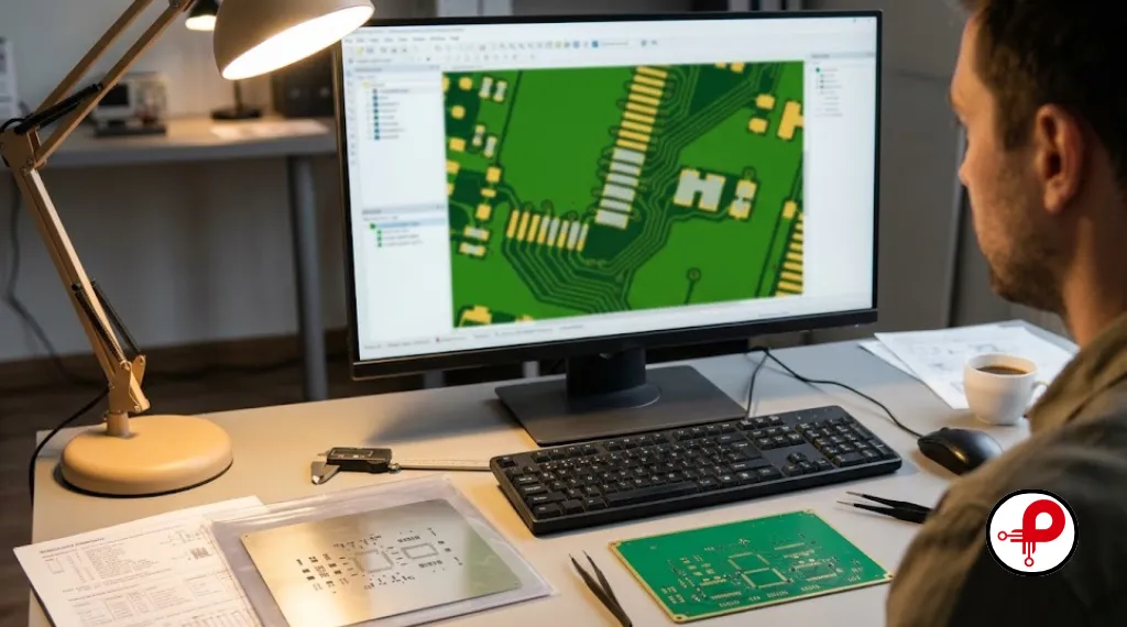
PCB stencil prices vary widely with size, type, frame and finishing.
How Much Does an SMT Stencil Cost?
In public listings checked for this guide, simple frameless prototype stencils from large online fabricators were offered for only a few dollars when ordered with boards. Specialist suppliers price higher. For example, one US stencil supplier listed its frameless prototype stencils from about $25 up to about $550 depending on size and options.
Framed production stencils, step stencils, electroformed stencils and special coatings all add cost. Always get a current quote from your PCB stencil manufacturer or service, because prices change often.
Ordering Checklist
Before you order a PCB stencil, confirm these details:
- Paste layer files: top and bottom paste Gerbers, plus the board outline.
- Stencil type: frameless for prototypes, framed for production printers.
- Thickness: chosen for your finest pitch part, for example 0.12 mm.
- Stencil size and frame size: match your printer or jig.
- Fiducials: half etched or marked on the stencil if your printer needs them.
- Sides: top only, bottom only, or both.
- Finishing: electropolishing or nano coating if you have fine pitch parts.
- Aperture changes: tell the supplier if you want them to apply their own aperture reductions, or if your paste layer is already final.
Ordering the stencil with your boards from the same fabricator is usually the easiest option, because they already have your files and can check alignment.
FAQ About PCB Stencils
1. What is a stencil in PCB?
↑2. What is the purpose of a PCB stencil?
↓3. How do you make a stencil for a PCB?
↓4. How thick is a PCB stencil?
↓5. How much does an SMT stencil cost?
↓6. Do you need a stencil for solder paste?
↓7. What are the common types of PCB stencils available?
↓8. What design rules determine if a PCB stencil will release paste properly?
↓Key Takeaways
A PCB stencil controls where solder paste goes and how much of it lands on each pad. Choose a frameless stencil for prototypes and a framed one for production. Pick the thickness for your finest pitch part, and check every small aperture against the area ratio of 0.66 and aspect ratio of 1.5.
Send clean paste layer files, print with one smooth stroke, and fix defects at the printing step before they become soldering problems. Do that, and your PCB stencil will give you clean, reliable joints on every board.